pcb-manufacturing-software
"PCB manufacturing software helps engineers design, test, and prepare printed circuit boards for production. It streamlines layout, routing, and fabrication processes, improves accuracy, and ensures designs meet manufacturing standards for quality and performance.


pcb-manufacturing-software
E N D
Presentation Transcript
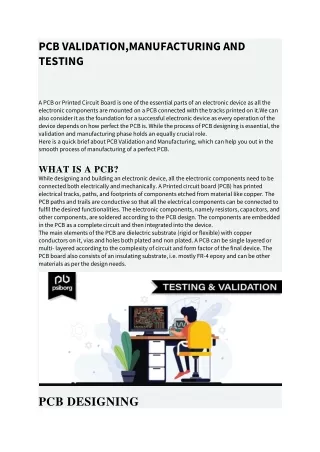
PCB Manufacturing Software: A Complete Guide for Engineers and Designers Printed circuit boards are at the heart of virtually every electronic device in the modern world — from smartphones and laptops to medical equipment and industrial machinery. Designing and manufacturing a PCB that performs reliably, meets tight tolerances, and can be produced efficiently at scale is a complex engineering challenge. The software tools used throughout this process play a critical role in determining whether a PCB project succeeds or fails. PCB manufacturing software encompasses a broad range of tools from electronic design automation platforms used during the schematic and layout phase, to computer- aided manufacturing software that translates designs into physical production instructions. Understanding what these tools do, how they fit together, and what to look for when choosing them is essential knowledge for anyone working in electronics design or manufacturing. 1. What Is PCB Manufacturing Software? PCB manufacturing software refers to the collection of digital tools used across the entire lifecycle of a printed circuit board from initial concept and schematic design through to layout, simulation, design rule checking, and the generation of manufacturing files. At the most fundamental level, it bridges the gap between an engineer's design intent and the physical production of a working board.
The software stack involved in PCB manufacturing typically includes electronic design automation tools for schematic capture and PCB layout, simulation software for signal integrity and thermal analysis, design rule check engines that verify the design against manufacturer constraints, and CAM software that prepares the final design files typically in Gerber format — for fabrication. Each stage is interconnected, and errors or inefficiencies at any point in the chain can have significant downstream consequences. 2. Electronic Design Automation (EDA) Tools EDA software is the foundation of any PCB project. These platforms allow engineers to create circuit schematics, build component libraries, design the physical PCB layout, and run preliminary electrical checks before the design goes anywhere near a factory. The quality and capability of the EDA tool you choose will have a direct impact on the complexity of designs you can handle, the accuracy of your output files, and the speed of your design iteration cycle. Some of the most widely used EDA platforms in the industry include: • Altium Designer: One of the most feature-rich and widely adopted professional EDA platforms, known for its powerful layout tools, integrated simulation capabilities, and strong component management features. It is a preferred choice for complex, high-layer-count designs. • KiCad: A free, open-source EDA suite that has grown enormously in capability and popularity in recent years. It is an excellent choice for hobbyists, startups, and small teams working on low-to-medium complexity designs. • Eagle (now part of Autodesk Fusion): A long-established PCB design tool that is particularly popular in the maker community and among engineers working on smaller, simpler boards. • Cadence Allegro: An enterprise-grade EDA platform used in high-speed and high-complexity designs, widely adopted in the semiconductor and telecommunications industries. • Mentor Graphics PADS: Another professional-tier platform known for its strong signal integrity tools and broad component library support. 3. Design Rule Check and Verification Software Before a PCB design is submitted for manufacturing, it must be verified against a comprehensive set of design rules. These rules define the minimum trace widths, clearances between copper features, via sizes, drill hole dimensions, and other physical parameters that the manufacturing process can reliably produce. A design rule check, or DRC, is an automated process that scans the entire layout and flags any violations of these constraints.
Most modern EDA platforms include built-in DRC engines, but dedicated verification tools offer more advanced capabilities — particularly for high-speed designs where signal integrity, electromagnetic compatibility, and thermal performance need to be validated alongside the basic geometric rules. Running thorough design rule checks before submitting a design for fabrication is one of the most important steps in avoiding costly respins and production delays. 4. Simulation and Analysis Software As PCB designs become more complex and operate at higher frequencies, simulation tools have become an indispensable part of the design process. Signal integrity simulation allows engineers to model how signals behave as they travel across the board — identifying issues such as reflections, crosstalk, and impedance mismatches before they cause problems in a physical prototype. Thermal simulation tools model heat distribution across the board and help engineers identify potential hotspots that could lead to component failure. SPICE-based simulation remains the industry standard for circuit-level analysis, while tools such as Ansys SIwave, Cadence Sigrity, and HyperLynx are widely used for board-level signal and power integrity analysis. Investing in simulation early in the design process reduces the number of physical prototypes required and significantly shortens the overall time to market. 5. CAM Software and Manufacturing File Generation Computer-aided manufacturing software is the final link between a completed PCB design and the fabrication facility that will produce it. CAM tools process the design files exported from the EDA platform — typically in Gerber RS-274X format along with an
Excellon drill file — and prepare them for the specific processes used by the manufacturer. This includes panelisation, the addition of tooling holes, copper balancing, and the generation of solder mask and silkscreen layers. Many PCB fabricators run their own proprietary CAM software internally, but designers can also use tools such as GerbMagic, CAM350, or the open-source FlatCAM to review and prepare their files before submission. Reviewing your Gerber files in a CAM viewer before sending them to the manufacturer is a critical quality control step that catches formatting errors, missing layers, and other issues that would otherwise only surface after the boards have been fabricated. 6. What to Look for When Choosing PCB Software With so many tools available, choosing the right software stack for your team and project type is an important decision. Key factors to consider include: • Design complexity support: Ensure the tool can handle the layer count, component density, and signal speeds your designs require. • Manufacturer compatibility: The software should export industry-standard file formats — particularly Gerber and ODB++ — that are accepted by your fabrication partners. • Component library quality: A large, well-maintained component library saves significant time during schematic capture and reduces the risk of footprint errors. • Collaboration features: For teams working across multiple locations, cloud-based or version-controlled workflows are increasingly important. • Cost and licensing model: Professional EDA tools can carry significant licensing costs. Open-source alternatives like KiCad offer a viable path for teams with tighter budgets. • Support and community: Strong documentation, active user communities, and responsive technical support are invaluable when working through complex design challenges. Final Thoughts PCB manufacturing software is not a single tool but an interconnected ecosystem of design, verification, simulation, and manufacturing preparation platforms. Choosing the right combination of tools — and understanding how they work together — is one of the most important investments an electronics engineer or design team can make. The right software stack reduces design errors, shortens development cycles, and ultimately leads to better, more reliable products reaching the market faster. Whether you are a solo engineer working on a first prototype or part of a large team producing complex, high-volume electronics, taking the time to evaluate and invest in the right PCB manufacturing software will pay dividends across every project you work on.