Download
1 / 3
0 likes | 1 Views
Semiconductor Inspection System Market

E N D
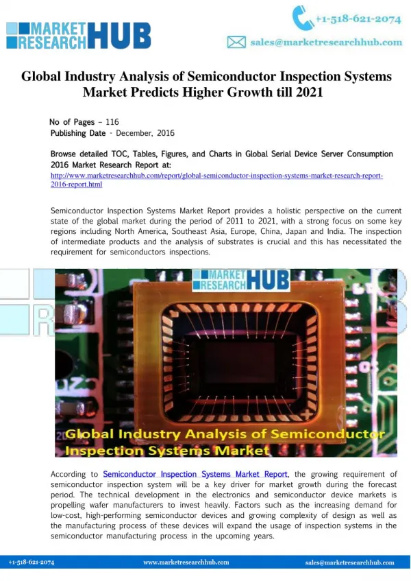
+1 217 636 3356 +44 20 3289 9440 sales@mobilityforesights.com Your Cart 0 Company Market Reports Consumer Research Advisory Services Exports - Imports Careers Contact Us Blog Your cart is empty Your Name Return to Shop Business Email Global Semiconductor Inspection System Market Size, Forecasts 2030 Country Phone Number +1 Company Name Single User License : $ 4,000 Your message Corporate User License : $ 6,000 By submitting this form, you are agreeing to the Terms of Use and Privacy Policy. Request Sample I'm not a robot reCAPTCHA Privacy - Terms BUY NOW DOWNLOAD SAMPLE DESCRIPTION TABLE OF CONTENTS SEMICONDUCTOR INSPECTION SYSTEM MARKET INTRODUCTION An inspection system is a set of processes and procedures used to evaluate the quality of a product or service. The goal of an inspection system is to identify defects and non-conformances so that they can be corrected or prevented. There are many different types of inspection systems, but they all share some common features. First, they all involve a set of criteria against which the product or service is evaluated. Second, they all involve a process for identifying defects and non- conformances. Third, they all involve a process for taking corrective or preventive action. Inspection systems can be either manual or automated. Manual inspection systems rely on human inspectors to identify defects. Automated inspection systems use machines to identify defects. Automated inspection systems are often more accurate than manual inspection systems, but they can be more expensive to implement. The benefits of an inspection system include:Improved quality: Inspection systems can help to identify defects and non- conformances so that they can be corrected or prevented. This can lead to improved product quality. Reduced costs: Inspection systems can help to reduce costs by identifying defects early in the production process. This can prevent costly rework and scrap. Improved customer satisfaction: Customers are more likely to be satisfied with products that are free of defects. Inspection systems can help to ensure that products meet customer expectations. 0 The challenges of an inspection system include:Cost: Inspection systems can be expensive to implement and maintain.Time: Inspection systems can add time to the production process. Continue Shopping Complexity: Inspection systems can be complex to design and implement.Accuracy: Inspection systems can be inaccurate, leading to false positives or false negatives. Overall, inspection systems can be a valuable tool for improving product quality and reducing costs. However, they should be carefully designed and implemented to avoid the challenges associated with them. A semiconductor inspection system is a device that uses optical, electrical, or mechanical methods to inspect semiconductor devices for defects. The system may be used to inspect a variety of semiconductor devices, including integrated circuits, transistors, and diodes. The inspection system typically consists of a light source, a detector, and a computer. The light source illuminates the semiconductor device, and the detector collects the light that is reflected or scattered from the device. The computer analyzes the data from the detector to identify defects in the device. Semiconductor inspection systems are used to ensure the quality of semiconductor devices. The systems can identify a variety of defects, including cracks, scratches, and foreign particles. The systems can also be used to measure the dimensions of semiconductor devices. Semiconductor inspection systems are an important part of the semiconductor manufacturing process. The systems help to ensure that semiconductor devices are free of defects, which can improve the performance and reliability of the devices. Here are some of the benefits of using a semiconductor inspection system:Improved product quality: Semiconductor inspection systems can help to identify and remove defects from semiconductor devices, which can improve the quality of the final product. Reduced costs: By identifying and removing defects early in the manufacturing process, semiconductor inspection systems can help to reduce the costs associated with scrap and rework.
Increased productivity: By improving the quality of semiconductor devices, semiconductor inspection systems can help to increase the productivity of the manufacturing process.Improved safety: By identifying and removing defects that could potentially cause safety hazards, semiconductor inspection systems can help to improve the safety of the manufacturing process. SEMICONDUCTOR INSPECTION SYSTEM MARKET SIZE AND FORECAST +1 By submitting this form, you are agreeing to the Terms of Use and Privacy Policy. The Global Semiconductor Inspection System Market accounted for $XX Billion in 2022 and is anticipated to reach $XX Billion by 2030, registering a CAGR of XX% from 2024 to 2030. SEMICONDUCTOR INSPECTION SYSTEM MARKET NEW PRODUCT LAUNCH The LS9600, a novel method for detecting particles and faults on non-patterned wafer surfaces, has been disclosed by Hitachi High-Tech Corporation. It incorporates a new high-output, short-wavelength laser that increases throughput at the sensitivity levels necessary for mass manufacture of cutting-edge semiconductor devices by about 2.6 times over previous generation systems. Hitachi High-Tech’s introduction of this product will assist to enhance yields and lower inspection costs connected with customers’ mass manufacture of semiconductor devices. Non-patterned wafer inspection systems are used for purposes such as regulating the state (cleanliness) of non-patterned wafers in semiconductor device production equipment to manage particles and flaws. Because semiconductor devices are shrinking, defects of interest (DOIs) affect yield during production. As a result, there is an increasing demand for high-sensitivity inspection capable of detecting DOIs as tiny as 20 nm throughout the whole surface of non-patterned wafers. Aside from high-sensitivity inspection to increase yield, there is also a considerable need for high throughput, which results in lower inspection costs. Improved scattered light data-processing methods provide increased sensitivity as well as increased throughput due to high- speed, real-time data processing. Hitachi High-Tech is working to meet customers’ various needs in processing, measurement, and inspection throughout the semiconductor manufacturing process by using this product, as well as wafer optical inspection systems and electron beam- based products such as a traditional CD-SEM(1) and DR-SEM(2). We will continue to offer novel and digitally upgraded solutions for goods for the foreseeable future. the forthcoming technological challenges, generate new value with clients, and contribute to cutting-edge production. (1) CD-SEM (Critical Dimension-Scanning Electron Microscope): This is a piece of equipment used to measure the tiny circuit patterns on semiconductor wafers. These systems, which are used for inspections on semiconductor device development and production lines, are critical for yield management. (2) DR-SEM (Defect Review-Scanning Electron Microscope): A device used to inspect tiny circuit patterns and flaws on semiconductor wafers. These systems, which are used for inspections on semiconductor device development and production lines, are critical for yield management. SEMICONDUCTOR INSPECTION SYSTEM MARKET COMPANY PROFILE Applied Materials KLA Corporation Nikon Metrology ASML Tokyo Electron Hitachi High-Technologies SEMICONDUCTOR INSPECTION SYSTEM MARKET THIS REPORT WILL ANSWER FOLLOWING QUESTIONS 1. How many Semiconductor Inspection Systems are manufactured per annum globally? Who are the sub-component suppliers in different regions? 2. Cost breakup of a Global Semiconductor Inspection System and key vendor selection criteria 3. Where is the Semiconductor Inspection System manufactured? What is the average margin per unit? 4. Market share of Global Semiconductor Inspection System market manufacturers and their upcoming products 5. Cost advantage for OEMs who manufacture Global Semiconductor Inspection System in-house 6. 5 key predictions for next 5 years in Global Semiconductor Inspection System market 7. Average B-2-B Semiconductor Inspection System market price in all segments 8. Latest trends in Semiconductor Inspection System market, by every market segment
9. The market size (both volume and value) of the Semiconductor Inspection System market in 2024-2030 and every year in between? 10. Production breakup of Semiconductor Inspection System market, by suppliers and their OEM relationship 11. RELATED REPORTS +1 By submitting this form, you are agreeing to the Terms of Use and Privacy Policy. Global LED Strip Lights Market Size and Forecasts 2030 Europe Gyroscope Sensor Market 2022- 2027 Europe Chemical Sensor Market 2022-2027 Global Methane Gas Sensor Market Size and Forecasts 2030 $4,000 Multi User $4,000 $4,000 $4,000 Multi User Multi User Multi User License - MARKET REPORTS CONSUMER RESEARCH INFORMATION ADVISORY SERVICES CONTACT INFORMATION 172/1, 2nd Floor, 5th Main, 9th Cross Automotive and Transportation About Us Focus Group Study Transaction Advisory Rd, Opposite to Kairalee Nikethan Semiconductor Our Clientele Education Trust, Indira Nagar 1st Stage, Ethnographic Market Positioning Agriculture and Construction Our People Bengaluru, Karnataka 560038, INDIA Research Assessment Equipment Blog Brand Awareness Custom Automotive Aerospace and Defense +1 217 636 3356, +44 20 3289 9440 Contact us Study Market Research Marine and Rail Terms & Conditions sales@mobilityforesights.com Consumer Satisfaction Strategic Advisory Logistics and Packaging Privacy Policy Survey Competitive Working Hours: Mon - Fri (9 AM - 9 PM Medical Devices ESOMAR Guidelines Consumer Expectation Intelligence IST) Chemical and Materials Compliant & Loyalty Assessment Electrical Machinery Connect with us ICT Energy, Power and Robotics New Technologies © Copyright 2017-2023. Mobility Foresights. All Rights Reserved.