Download
1 / 20
200 likes | 579 Views
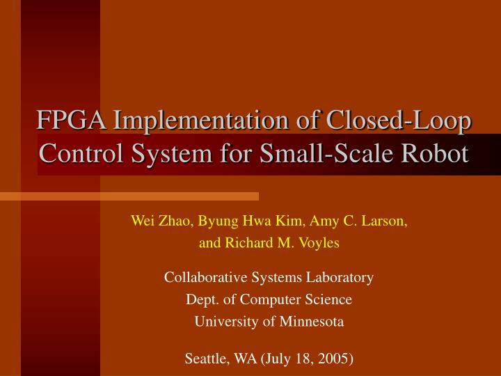
FPGA Implementation of Closed-Loop Control System for Small-Scale Robot. Wei Zhao, Byung Hwa Kim, Amy C. Larson, and Richard M. Voyles Collaborative Systems Laboratory Dept. of Computer Science University of Minnesota Seattle, WA (July 18, 2005).

E N D
FPGA Implementation of Closed-Loop Control System for Small-Scale Robot Wei Zhao, Byung Hwa Kim, Amy C. Larson, and Richard M. Voyles Collaborative Systems Laboratory Dept. of Computer Science University of Minnesota Seattle, WA (July 18, 2005)
Small-scale robot for urban search and rescue Bore Hole Search Occluded Spaces with Tethered Robot Dropped Through Bore Hole Deployed Configuration Stowed Configuration Department of Electrical Engineering, University of Minnesota
Introduction • Small-Scale Robot • Beneficial for urban search and rescue, military surveillance and countermeasure, planetary exploration • Resource-constrained issues • Mechanical design and controller design CRAWLER functional architecture Department of Electrical Engineering, University of Minnesota
Introduction (cont’d) • Tasks of this project • Investigate FPGA implementation of different designs for PID control system to provide performance and resource requirements to Run Time Reconfiguration (RTR) and HW/SW codesign algorithms • Different designs • One-channel parallel and serial designs • Multiple-channel designs • These designs are evaluated in terms of • Area • Power • Speed Department of Electrical Engineering, University of Minnesota
Related work • Weiss et al. analyzed different RTR methods on the XC6000 architecture [2]. • Shirazi described a framework and tools for RTR [5]. • Noguera and Badia proposed a HW/SW codesign algorithm for dynamically reconfiguration [3]. • Chen et al. implemented a complete wheelchair controller on an FPGA with parallel PID design [13]. • Samet et al. designed three PID architectures for FPGA implementation – parallel, serial and mixed [14]. • Chan et al. implemented power-efficient design of PID controller using FPGA [Chan04]. • [Chan04]: Y.F. Chan, M. Moallem, and W. Wang, “Efficient implementation of PID control algorithm using FPGA technology,” in 43rd IEEE Conference on Decision and Control, Vol. 5, Dec. 2004, pp. 4885 – 4890. Department of Electrical Engineering, University of Minnesota
PID control algorithm • Differential equation Kp : proportional gain, Ti : integral time constant, Td : derivative time constant • Difference equation : Positionalgorithm : Incrementalalgorithm where Department of Electrical Engineering, University of Minnesota
One-channel parallel design • Incremental algorithm 4 additions and 3 multiplications Department of Electrical Engineering, University of Minnesota
One-channel serial design Department of Electrical Engineering, University of Minnesota
Multiple-channel designs • Channel-level parallel (CLP) designs • Each channel has its own PID unit • Large area, proportional to number of channels • Channel-level serial (CLS) designs • All channels share one PID unit • Small area independent of each channel • More complex control unit • Context switching Department of Electrical Engineering, University of Minnesota
Multiple-channel designs • Channel-level parallel (CLP) designs • Each channel has its own PID unit • Large area, proportional to number of channels • Channel-level serial (CLS) designs • All channels share one PID unit • Small area independent of each channel • More complex control unit • Context switching Arithmetic-level parallel (ALP) design Arithmetic-level serial (ALS) design Department of Electrical Engineering, University of Minnesota
Experiment system platform • FPGA board (Xport) • Spartan II XC2S150 FPGA • Microprocessor module (GBA) • ARM7TDMI processor, 32-bit RISC Department of Electrical Engineering, University of Minnesota
Function test • Step response control • All designs perform correct function. • Fast response, small overshoot and high accuracy. Department of Electrical Engineering, University of Minnesota
Performance test: area • Area test • Test tool • Xilinx ISE, Place & Route Report • Test metric • CLB slices • Logic gates Device resources utilization of designs Department of Electrical Engineering, University of Minnesota
Performance test: area (cont’d) • Area • CLS design smallerthan CLP design for large number of channels • But, CLP design smaller for small number of channels • Arithmetic-level serial design always smaller than arithmetic-level parallel, whatever CLP or CLS Department of Electrical Engineering, University of Minnesota
Performance test: speed • Speed test • Test tool • Xilinx Timing Analyzer Department of Electrical Engineering, University of Minnesota
Performance test: power • Power test • Test tool • Xilinx XPower • Input signals • Set input signal frequency and activity rate: far from accurate • Simulation data file (VCD file): accurate • Simulation tool: ModelSim • Simulation input: real step response experiment data • Two situations • Stable state • Control error = 0 • Dynamic state • Control error 0 Department of Electrical Engineering, University of Minnesota
Performance test: power (cont’d) Department of Electrical Engineering, University of Minnesota
Performance test: power (cont’d) • Power dissipation • For the same sampling frequency, CLP+ALS design consumes least power. • But area of CLP is too large for large number of channels. CLS+ALS design has smallest area. Department of Electrical Engineering, University of Minnesota
Conclusions • Preliminary work exploring resources-constrained robot control system design using FPGA. • One-channel serial and parallel architectures, and CLS multiple-channel designs for PID closed-loop control. • Functional correctness verified. • For one channel design increasing sampling frequency, • ALS shows less power than ALP. • For small number of channels • CLP+ALS design has smallest area and least power. • For large number of channels • CLP+ALS design still least power, but design is too large. • CLS+ALS design has smallest area. • Performance test methodologies and metrics discussed. Department of Electrical Engineering, University of Minnesota
Future work • Implement and test on Virtex-II Pro FPGA. • Run time reconfiguration: reconfigure structure to adapt different situation and terrain. • Use Virtex-II FPGA clock gating structure to improve power efficiency. • Decrease motor power consumption. • Current work: develop FPGA Interface to C3088 camera using Xilinx ML310 board (Virtex-II pro). Department of Electrical Engineering, University of Minnesota