Download
1 / 46
1.32k likes | 4.08k Views
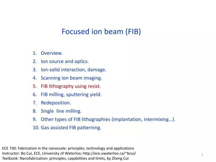
Focused ion beam (FIB). Overview. Ion source and optics. Ion-solid interaction, damage. Scanning ion beam imaging. FIB lithography using resist. FIB milling, sputtering yield. Redeposition. Single line milling. Other types of FIB lithographies (implantation, intermixing…).

E N D
Focused ion beam (FIB) Overview. Ion source and optics. Ion-solid interaction, damage. Scanning ion beam imaging. FIB lithography using resist. FIB milling, sputtering yield. Redeposition. Single line milling. Other types of FIB lithographies (implantation, intermixing…). Gas-assisted FIB patterning. ECE 730: Fabrication in the nanoscale: principles, technology and applications Instructor: Bo Cui, ECE, University of Waterloo; http://ece.uwaterloo.ca/~bcui/ Textbook: Nanofabrication: principles, capabilities and limits, by Zheng Cui
Focused ion beam (FIB) lithography overview • FIB lithography resembles e-beam lithography, but with more capabilities: • Write pattern in a resist, like EBL. • Etch atoms away locally by sputtering, with sub-10nm resolution (subtractive), most popular application of FIB. • Deposit a material locally, with sub-10nm resolution (additive). • Ion implantation to create an etching mask for subsequent pattern transfer. • Material modification (ion-induced mixing, defect pattern…). • Simultaneous observation of what is happening for resist-less lithography (i.e. local etch and deposit).
Pretty fast beam-blanker, though for advanced EBL, it can be 50MHz. This project didn’t achieve its goal. FIB can by no means replace EBL. http://www.nanofib.com/
Comparison: EBL and FIB lithography (with resist) Like EBL, ion-matter interaction can also generate low-energy secondary electrons, which can expose the resist for lithography. Naturally, in principle all EBL resists can also be used as FIB lithography resist. • Proximity effect of FIB lithography is negligible, no electron backscattering. • Forward scattering is also weaker. • This means writing pixel size beam spot size, beam blanker may not follow. (For EBL, pixel size >> beam spot size, exposure by proximity effect.) • For the same beam spot size, higher resolution than EBL, due to shorter ion range, smaller lateral straggling, weaker secondary electron generation, lower energy of secondary electrons. • Greater resist sensitivity than EBL that increases throughput. Ion-beam electron-beam
Comparison: EBL and FIB lithography (with resist) • However, it is more difficult to focus ion beam (chromatic aberration, no magnetic lens…). • So one must use low beam current for the same resolution, which offset its high sensitivity and reduces writing speed. • Impurity of source ions within resist is an issue. • The biggest disadvantage of FIB lithography: limited exposure depth in resist (<100nm for 100keV); thin resist makes following liftoff or etching process difficult. Spot size of a FEI FIB system. (Spot size for EBL can be <10nm at current several nA)
Comparison to EBL: resist sensitivity PEB: post exposure bake SAL-601: High sensitivity (10C/cm2) chemically amplified negative resist, with good resolution (sub-100nm), high contrast, and moderate dry etch selectivity. But not so stable with short shelf lifetime. http://snf.stanford.edu/Process/Lithography/ebeamres.html • Very high ion beam energy (260kV), so this comparison of sensitivity may not be typical. • Here the resist sensitivity is about 2 orders higher than that of EBL.
Focused ion beam (FIB) Overview. Ion source and optics. Ion-solid interaction, damage. Scanning ion beam imaging. FIB lithography using resist. FIB milling, sputtering yield. Redeposition. Single line milling. Other types of FIB lithographies (implantation, intermixing…). Gas-assisted FIB patterning.
FIB milling • Sputter process. • Less damage at cutting surface for small currents. • Resolution better for small current but high currents mill faster - use series of decreasing currents. • Significant redeposition - milling strategy is important. • High depth of focus (ion shorter wavelength than electron) – mill features with high aspect ratio, rough surface OK. • Coupling with SIMS gives in-situ information on chemical content.
Sputtering by ion beam • Sputtering rate depends on ion energy, mass, crystal orientation, substrate nature. • One Ga ion of energy 30 keV sputters a few atoms from Si surface. • Sputtered feature is broader than beam size: 10nm beam causes 20 to 30 nm sputtered recess. • With a 1nA ion beam current, sputtering 1μm3/sec. • Optimal ion energy 10-100keV. • Higher energy leads to more implantation. • For energy >1MeV, backscattering and nuclear reaction become dominant.
Materials modification with ion beams 0-1 eV: adsorption Rp ≈ 0 Chemistry: (several eV) 15-102eV: atomic displacements Rp ≈ 1-10 nm 103-105eV: dense cascades, local melting Rp ≈ 10-1000 nm Physics: (101-107eV) 106-109eV: no-collisions, electronic excitation Rp ≈ 1-100 μm
Sputtering yield Y = number of recoiling atoms out of the target surface per incident ion = 1-50 Sputtering yield is correlated with melting point.
Sputtering yield of different material • Sputtering yield varies with material, orders of magnitude difference across periodic table. • Sputter rate (m3/sec) = yield(atoms/ion) flux(# of ions/sec)/number density(atoms/m3). • Actual rate much lower due to re-deposition of sputtered material.
Energy dependence of sputtering yield Ar: Z=18 Ga: Z=31 As: Z=33 As/Au Ga/Au Ar/Au As/Si Ga/Si Sputter yield “saturates” at 100keV, higher energy leads to significant implantation “Recent developments in micromilling using focused ion beam technology”, Tseng, 2004
Angular dependence of sputtering yield Au sputtering rate is less angle-dependent than Si. Au Si 90keV 30keV • Maximum sputter yield at 75-80o. • However, FIB milling is usually done at normal incidence for vertical trench profile. • Actually no longer “normal” once milling started – inclined incidence on tapered sidewall.
Rate of material removal: constant dose different materials Constant dose of 7.51012Ga+, delivered with 1nA beam current. • Ga ion into Zn, Cu, Al, and Si at normal incidence. • SEM cross sections at 90o tilt. • Trench depth varies with material. • Zn has highest sputtering rate. • Cu shows topography formation. • Si has smoothest crater bottom. Brenda Prenitzer, University of Central Florida, PhD dissertation (1999).
Steady state ion implantation Implant profile with steady state sputtering Implant profile if without sputtering Increasing dose does not implant more ions to the surface, but rather, only recedes the “same” steady state surface with time.
Effect of incidence angle Ion • Asperities on a surface will be FIB milled at different rates due to topographic effects on milling • The topographic effects will grow and exacerbate as FIB milling continues • This is why (even for normal ion incidence) surfaces are “never” FIB milled from top-down; but rather, are created by FIB milling at high incident angles (as if milling from sidewall and propagate along beam).
Charging effect when milling insulator Charging can be eliminated by electron beam bombardment of surface. (most FIB is equipped with SEM – DualBeam system)
Channeling effect when milling crystalline material Box milling of poly crystalline material (steel), rough surface. Box milling of poly crystalline Cu. Channeling effect suppressed by doping with impurity atoms that block the ion channels.
Focused ion beam (FIB) Overview. Ion source and optics. Ion-solid interaction, damage. Scanning ion beam imaging. FIB lithography using resist. FIB milling, sputtering yield. Redeposition. Single line milling. Other types of FIB lithographies (implantation, intermixing…). Gas-assisted FIB patterning.
redeposition Scanning beam Re-deposition • Redeposition depends on: • Kinetic energy of atoms leaving surface • Sticking coefficient of target • Sputtering yield of target • Geometry of feature being milled • Factors that increase sputtering rate tend to increase redeposition: • Beam current • Incident ion kinetic energy • Incident ion attack angle • Target material properties Scan direction 2m Si milled by 30keV Ga+, slow single pass at 2s per line with 300 scan lines.
Geometry effect of re-deposition Constant dose variable area, milling of (100) Si at normal incidence with 1.5x10¹¹Ga+/μm3. Slope of sidewall increases (less steep) as trench width decreased, as sputtered atoms have less chance to get out of the trench. B. Prenitzer, Univ. Cent. Florida dissertation (1999)
Effect of beam current on re-deposition 500pA 1000pA 2000pA Cu (110) Si (100) 10m For higher beam current, re-deposition increase, sidewall definition worse. For Cu, rough surface at all beam currents.
Effect of scan sequence BK7 glass Milled from center to edge Milled from edge to center The earlier the region is milled, the more re-deposited material is accumulated there. “Recent developments in micromilling using focused ion beam technology”, Tseng, 2004
How to deal with re-deposition Si milled by 30keV Ga+, total dose 1.91018 ions/cm2. Fast 200 repetitive passes at 10ms per line with 300 scan lines. Slow single pass at 2s per line with 300 scan lines. “Characteristics of Si removal by fine focused gallium ion beam”, Yamaguchi, JVST, 1985.
How to deal with re-deposition, another example Parallel: mill all pixels to a small depth, then return to mill deeper … until targeted depth achieved, re-deposited material milled away by following mills. Serial: mill each pixel all the way through before milling the next, re-deposited material covers holes milled previously. • Summary for minimizing re-deposition effect: • Mill large and less critical pattern first, using high beam current. • Use multiple passes, not single pass. • Mill fine and critical pattern last, using low beam current and multiple pass.
Focused ion beam (FIB) Overview. Ion source and optics. Ion-solid interaction, damage. Scanning ion beam imaging. FIB lithography using resist. FIB milling, sputtering yield. Redeposition. Single line milling. Other types of FIB lithographies (implantation, intermixing…). Gas-assisted FIB patterning.
Pixel size vs. beam size Ion flux distribution along a scan line with pixel/diameter=1.5 (top), 3.0(bottom) As a rule, for continuous non-wavy milling, pixel spacing/beam diameter 1.5 “Recent developments in micromilling using focused ion beam technology”, Tseng, 2004
Channel milling using single pass Channel profile by AFM redeposition Milled into Au by 90keV As2+ FIB with 5ms dwell time. I=5pA, pixel spacing 14.5nm, beam diameter 50nm. Single pass, aspect ratio 1/3 and is insensitive to dwell time. • Due to re-deposition, channel depth cannot be calculated simply by sputter yield. • V-shaped channel profile is the inherent shape obtained by single-pass FIB milling. • At long dwell time, the mouth width of the channel (B) can be one order larger than beam size, because the “tail” of the beam can mill sizable amount material.
Channel milling using single pass Relationship between feature size (depth by milling and etching or height by swelling and deposition) and ion doses for various ion species and materials. Dwell time ion dose D Almost universally log(M)=a+blog(D) M is milling depth or any feature size in milling experiment. Then milling yield: Y=dM/dD=b(M/D)
How to mill high aspect ratio narrow trench FIB milled trenches in ta-C film using beam current (from left to right) of 32, 3, 3, 32, 7, 7, 32 and 32 pA, respectively. Trenches with width 30–40 nm, aspect ratio up to 25, beam current 1.8-3pA For high aspect ratio, use small beam current and large number of repetitive passes. “Focused ion beam patterning of diamond-like carbon films “, Stanishevsky, 1999.
Focused ion beam (FIB) Overview. Ion source and optics. Ion-solid interaction, damage. Scanning ion beam imaging. FIB lithography using resist. FIB milling, sputtering yield. Redeposition. Single line milling. Other types of FIB lithographies (implantation, intermixing…). Gas-assisted FIB patterning.
Patterning etching mask by ion implantation • High concentration p+ doping in Si drastically reduces the etch rate by KOH. • The implantation depth is roughly 1nm/keV (e.g. 30nm for 30keV Ga+ ion). • The critical dose for the etch mask to be effective is 11015 ions/cm2 (=160C/cm2=10 ions/nm2). • The implanted region is completely amorphous (amorphization dose is 11014 ions/cm2). • At higher doses such as 11016 ions/cm2, sputtering (milling) of sample surface becomes significant. Fabrication of cantilevers by shallow doping (left-hand side) and milling and sidewall doping (right-hand side): (a) FIB exposure (milling and/or implantation), (b) during KOH etching and (c) after etching is completed. Reyntjens and Puers, “A review of focused ion beam applications in microsystem technology”, J. Micromech. Microeng. 11, 287-300 (2001).
FIB implantation and pattern transfer: results Nano-cup by extending vertical FIB milling to several m. SEM photomicrographs of cantilevers (2 μm long, 100 nm wide and 30 nm thick). Tseng, “Recent developments in nanofabrication using focused ion beams”, Small, 1(10), 924-939 (2005).
FIB implantation and pattern transfer: results • Rounded (wider interior, narrower near surface ) groove array fabricated by Si-FIB implantation on AlGaAs substrates. • Si+ ion implantation at 200keV energy, high energy leads to large grooves. • Hot (70oC) HCl etches highly doped (1000 ions/nm) region much faster. • Implantation can also irradiating polymer resist materials to increase its etching resistance. • Here 30 keVGa+ FIB with 117C/cm2 doses to make implanted patterns in Shipley SPR660 positive photoresist layers. • Ga2O3 is formed that can be used as RIE etch mask using O2 plasma. FIB images of double 100 nm (left) and 30 nm (right) lines patterned by FIB implantation in SPR660 photoresist after O2 RIE.
Ion beam lithography on AlF3 resist AlF3: inorganic e-beam lithography resist. Form F2 gas upon exposure, leaving behind Al. High-resolution direct machining: FIB etched lines on AlF3(50nm)/GaAs, ion dose 92nC/cm. The edges of the resist etched layer appear transparent and the lines in GaAs display a very reproducible width of 8nm. Explanation of this high resolution: flux-dependent vaporization of AlF3, which is acting as a filter versus the tails of the ion-probe current distribution. AlF3 inorganic resist using 30kV Ga ion, large features, pitch 1m. “Nano-fabrication with focused ion beams”, Microelectronic Engineering 57–58, 865–875 (2001)
Ion beam lithography on Au55(PPh3)12Cl6 resist Au55(PPh3)12Cl6: ion-sensitive negative resist, though recoil atoms and secondary electrons induced by recoils of light atoms in the resist also plays a role for resist exposure. AFM image of a typical gold-containing butterfly-type pattern, realized by FIB irradiation of a single solid Au55(PPh3)12Cl6 resist layer. Dose on big pad is 1014 ions/cm2. The 3D connecting channel with granular morphology is clearly shown: width 30nm; height 20nm; length 1.5m. (Ga ions, energy 30keV, initial thickness for gold cluster compound 50nm) “Nano-fabrication with focused ion beams”, Microelectronic Engineering 57–58, 865–875 (2001)
Ion beam induced intermixing Faraday microscopy image of magnetic patterns of a FIB dot array (Ga ions, 28 keV). (either bright or dark region is irradiated) Initial film: Pt(3.4nm)/Co(1.4nm, ferromagnetic)/Pt(4.5nm). Mechanism: ion-induced atom displacement at the Co/Pt interfaces (ion beam mixing effect). paramagnetic Faraday ellipticity loops obtained at room temperature after uniform Ga irradiation. Irradiation reduces coercivity; at even higher dose 21015, the film becomes paramagnetic.
Ion beam patterning of HOPG HOPG: a kind of graphite, highly oriented pyrolitic graphite. TM-AFM images (980 nm × 980 nm) of the morphologies of defects created by FIB on a HOPG substrate (35keV Ga+ ions, probe size 6nm, ion dose 3750 ions/pt. The surface bumps are organized in a matrix of periodicity Ldef=250nm, note the very reproducible height (around 1.8nm) of the fabricated structures. For lower ion doses (as here), only ion-induced defects and subsequent local volume variations corresponding to surface modification are evidenced. For higher ion doses, holes are etched into the sample, leading to a volcano-crater like morphology. Use irradiated HOPG substrate to guide the deposition of metal clusters. TM-AFM (2μm × 2μm) image of morphologies of HOPG surfaces. After deposition of gold clusters. After deposition of Co50Pt50 followed by a thermal annealing.
Focused ion beam (FIB) Overview. Ion source and optics. Ion-solid interaction, damage. Scanning ion beam imaging. FIB lithography using resist. FIB milling, sputtering yield. Redeposition. Single line milling. Other types of FIB lithographies (implantation, intermixing…). Gas-assisted FIB patterning.
Gas-assisted FIB lithography FIB alone capabilities FIB with gas Enhanced etching Ion Etching Poor selective Etching Selective etching Material deposition Ion deposition
Gas-enhanced FIB milling (etching) • Impinging Ga+ knocks out atoms and ions from sample • Redeposition is prevented by chemical reaction with the adsorbed gas - formation of volatile species. • Etching gases that react only with certain species - selective milling • Examples of etching gases • XeF2 enhances Si and insulator milling. • Cl2, Br2, I2 enhances metal milling. • H2O enhances carbon (polymers, ...) milling. Sputtering yield enhancement factors
Gas-enhanced FIB milling (etching) • Adsorption of the gas molecules on the substrate • Ion bombardment ionize the absorbed gas atoms, making them reactive. • Interaction of the gas molecules with the substrate • Formation of volatile species: GaCl3, SiCl4, SiF4 • No chemical reaction • Formation of non-volatile species: AlF3, oxide layer • Evaporation of volatile species and sputtering of non volatile species
Gas-assisted selective/enhanced FIB milling Selective etching using XeF2 Al SiO2 With XeF2 Without XeF2 Enhanced etching using XeF2 Orsay Physics