Download
1 / 14
140 likes | 260 Views
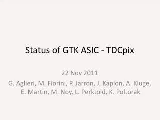
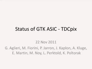
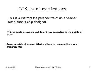
Status of GTK ASIC - TDCpix. G. Aglieri, M. Fiorini, P. Jarron, J. Kaplon, A. Kluge, E. Martin, M. Noy, L. Perktold, K. Poltorak. TDCpix ASIC block diagram (60 bit serial/4 LVDS pairs parallel). 45. August 7, 2012. 4x45. 45. 2.7 /4 Mhits/s. Config pixel. 5 bit trimDAC. pixel.

E N D
Status of GTK ASIC - TDCpix G. Aglieri, M. Fiorini, P. Jarron, J. Kaplon, A. Kluge, E. Martin, M. Noy, L. Perktold, K. Poltorak
TDCpix ASIC block diagram (60 bit serial/4 LVDS pairs parallel) 45 August 7, 2012 4x45 45 2.7 /4 Mhits/s Config pixel 5 bittrimDAC pixel driver&line&receiver pixel cell x 45 pixel column double column 0 column 1 double column 5 double column 4 double column 3 double column 1 double column 6 double column 2 double column 19 end of column 5 2, parallel_load&daq_rdy hitArbiter 0 & edge detector hA 1 hA 8 hA 2 column 0 1,hit 32 clkdll=320MHz coarseTimeStamp DLL fineHitRegister 0 coarseHitRegister 0 DLL 0 2 x 32 2 x (13 + 5) 5 add+5 pil serialTime state machine 12 1 > CP&PD clksync or clkserialTime syncRegister 2 x 32 2 x (13 + 5) 5 add+5 pil clkdll coarseTimeStampServer0 > 9 fineTimeStampEncoder coarseTimeStampEncoder group EOC 1 group EOC 2 group EOC 8 group EOC 0 5 rise+5 trail 13 rise+5 trail 5 address + 5 pileup 32 fineRise 32 fineTrail 2x12+1 coarseRise 2x4+1 coarseTrail 5 fineRise 5 fineTrail 12+1 coarseRise6+1 coarseTrail 2 group collision > clksync 0.3/0.44 Mhit/s pixelGroupFifo (depth= 3) 648 FF @ 2 depth 8 bit thresholdDACcolumn & 3 bit bias DAC 42 42 5 rise+5trail+12+1 rise+6+1 trail+5add+5pil+2col=42 42 columnMux 9 to 1 23 cell units * (0.40 µmx 4.8 µm)* (648+152+373/10) FF=37000 µm2=124µm*300µm ConfigDoubleCol 42+4 add=46 2.7/ 4 Mhit/s columnFifo (depth= 6) columnFifoController clksync > 152FF @ 4 depth 7x12+1x6 46 46 quarterchipFifo&frameInserter Controller > clksync & enableclk sync register 90 clksync quarterChipMux 10 to 1 serialTimeMux 90 to 48 > clksync 48 46+4 add=50 quarter chip RO 0 quarter chip RO 3 quarter chip RO 2 quarter chip RO 1 data formatter & comma & frame inserter 48 min. 40 FIFOs 1 FIFO overflow bit, optional overflow count > > clksync & enableclk clksync & enableclk 8b10b encoder sync register 60 > > clkserial/2 serializer controller clkserial/2 clkmultiserial 27/ 40 Mhit/s parallelOut > 2 58 0 clkserial/2 serializer FIFO overflow status > 3 59 1 2.4/3.2 Gbits/s CML driver 4 x SLVS480/640 Mbit/s multiSerialPower clkmultiserial path d is doubled as to have one direct link from clkserial/2 to clkfiforead clkFIFOread 2 world clkserial/2 clksync global DACs clkmultiserial or clktest clkSerial=2.4/ 3.2 GHz c /2 /2 /5 /6 /2 /8 9+1x temp 0 1 band gap bandgap override 1 0 PLL /6 1 0 /5 reset_corsecnt SLVS reset_global SLVS 0 0 PLL override e 2 (1 temp) 1 1 ext 1 a b c d config/statuschip 0 analogMonitorMux clkconfig test pulse b d f muxmode clkDigital=320/ 480 MHz > clkconfig SLVS320 MHz qchip clock divider & clk distribution SLVS≥320 Mbit/s 3 clkDll SLVS SLVS analog DC CMOS DC PLL SLVS 320/480MHz is located in synchronous logic; clk divider needs synchronous reset with respect to receiving clock domain (clkmultiserial) avg. nominal rate (750 MHz beam (104 Mhit/s per chip) / rate with 2.4 Gbiit/s serializer [Mhit/s])
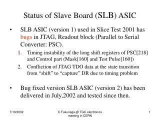
12000 µm Column 0 Corners: 125 µm Pixel = column * 45 + row Pixel group = column * 9+ group group 0 contains pixel 0 Pixel matrix: 13500 µm row 0 Band Gap 1100x400 Test pads 215x700 qchip 3 3000x500 qchip 2 3000x500 qchip 1 3000x500 qchip 0 3000x500 clk buffer & reset buffer & 20 clk dll buffers 12000 x 40 config 12000 x 300 Bgana 1400x300 Bgdig&temp 1500x300 PLL & 4 x Serializer & clk divider 8400 x 500 IO row 12000 x 400 (158 pads)
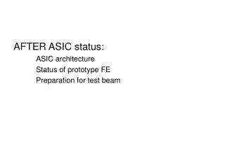
12000 µm Column 0 Corners: 125 µm row 0 Pixel = column * 45 + row Pixel group = column * 9+ group group 0 contains pixel 0 Pixel matrix: 13500 µm double column analog 0 double column analog 19 EoColumn bias 1800 µm TL rx: 70 µm double col. dig.0 double col. dig.19 hitArbiter & DLL, SM, fine registers & Coarse units, pixel group FIFOs, column FIFO 2477 µm Test pads 215x500=9 pads Quarter chip read-out 500 µm qchip 2 3000x500 qchip 1 3000x500 qchip 3 3000x500 qchip 0 3000x500 qchip & qconfig 3 3000x500 Clk_dll & reset_cc 72 µm clk buffer & reset buffer & 20 clk dll buffers 119000 x 72 Test pulse distributor 72 µm test pulse distributor 11900 x 72 config 11900 x 292 Configuration 292 µm BGana 1400x300 Bgdig&temp 1500x300 Serializer & PLL 500 µm PLL & 4 x Serializer & clk divider 8400 x 500 IO row 12000 x 400 (158 pads) IO row ~400 µm Total: > 19683 µm
serialPLL2_4lowClkSync = “001010 ext320highClkSync=“H100H0” H/L don’t care serialPLL2_4HighClkSync = “000010” ext480lowClkSync=“H110H1” H/L don’t care serialPLL3_2= “001000” ext480highClkSync=“H100H1” H/L don’t care clkmultiserial clkmultiserial clkmultiserial clkmultiserial clkmultiserial clkmultiserial clkmultiserial clkmultiserial path d is doubled as to have one direct link from clkserial/2 to clkfiforead path d is doubled as to have one direct link from clkserial/2 to clkfiforead path d is doubled as to have one direct link from clkserial/2 to clkfiforead path d is doubled as to have one direct link from clkserial/2 to clkfiforead path d is doubled as to have one direct link from clkserial/2 to clkfiforead path d is doubled as to have one direct link from clkserial/2 to clkfiforead path d is doubled as to have one direct link from clkserial/2 to clkfiforead path d is doubled as to have one direct link from clkserial/2 to clkfiforead clkFIFOread clkFIFOread clkFIFOread clkFIFOread clkFIFOread clkFIFOread clkFIFOread clkFIFOread clkserial/2 clkserial/2 clkserial/2 clkserial/2 clkserial/2 clkserial/2 clkserial/2 clkserial/2 clksync clksync clksync clksync clksync clksync clksync clksync clkSerial=2.4/ 3.2 GHz clkSerial=2.4/ 3.2 GHz clkSerial=2.4/ 3.2 GHz clkSerial=2.4/ 3.2 GHz clkSerial=2.4/ 3.2 GHz clkSerial=2.4/ 3.2 GHz clkSerial=2.4/ 3.2 GHz clkSerial=2.4/ 3.2 GHz c c c c c c c c /2 /2 /2 /2 /2 /2 /2 /2 ext320lowClkSync=“H110H0” H/L don’t care /5 /6 /5 /6 /2 /2 /2 /6 /6 /5 /5 /2 /6 /2 /6 /5 /5 /6 /5 /2 /6 /5 /2 /2 /2 /2 /2 /2 /2 /2 /2 /2 /8 /8 /8 /8 /8 /8 /8 /8 0 0 0 0 0 0 0 0 1 1 1 1 1 1 1 1 1 1 1 1 1 1 1 1 Modes: serialPLL2.4/serialPLL3.2/ext320/ext480/PLLoverride abc: /001010/110*010/111*011/101*010 8 modes = 3 bits clkInDigital=20/26.66/320/480/320MHz clkPLL=2.4/3.2/-/-/0.32GHz clksync=240(10)/ 320(10)/ 320*(0)/240*(2)/32(1) MHz clkFIFOread=40(60)/53(60)/27(12)/40(12)/5.3 MHz(60) clkmultiserial=480/640/320/480/64 MHz clkconfig=320/320/320/240/320 MHz ? if PLL runs on 480?? () =division factor, * can also be 0 or 1 to change clksync in TDC 0 0 0 0 0 0 0 0 PLL PLL PLL PLL PLL PLL PLL PLL PLLoverride320=“101010” H/L don’t care /6 /6 /6 /6 /6 /6 /6 /6 1 1 1 1 1 1 1 1 0 0 0 0 0 0 0 0 /5 /5 /5 /5 /5 /5 /5 /5 0 0 0 0 0 0 0 0 0 0 0 0 0 0 0 0 PLL override PLL override PLL override PLL override PLL override PLL override PLL override PLL override e e e e e e e e 1 1 1 1 1 1 1 1 1 1 1 1 1 1 1 1 ext ext ext ext ext ext ext ext 1 1 1 1 1 1 1 1 a a a a a a a a b b b b b b b b c c c c c c c c d d d d d d d d 0 0 0 0 0 0 0 0 clkconfig clkconfig clkconfig clkconfig clkconfig clkconfig clkconfig clkconfig b b b b b b b b d d d d d d d d f f f f f f f f muxmode muxmode muxmode muxmode muxmode muxmode muxmode muxmode clkDigital=320/480 MHz clkDigital=320/480 MHz clkDigital=320/480 MHz clkDigital=320/480 MHz clkDigital=320/480 MHz clkDigital=320/480 MHz clkDigital=320/480 MHz clkDigital=320/480 MHz qchip clock divider & clk distribution qchip clock divider & clk distribution qchip clock divider & clk distribution qchip clock divider & clk distribution qchip clock divider & clk distribution qchip clock divider & clk distribution qchip clock divider & clk distribution qchip clock divider & clk distribution 3 3 3 3 3 3 3 3 LVDS+2CMOS LVDS+2CMOS LVDS+2CMOS LVDS+2CMOS LVDS+2CMOS LVDS+2CMOS LVDS+2CMOS LVDS+2CMOS CMOS DC CMOS DC CMOS DC CMOS DC CMOS DC CMOS DC CMOS DC CMOS DC PLL PLL PLL PLL PLL PLL PLL PLL LVDS 320/480MHz LVDS 320/480MHz LVDS 320/480MHz LVDS 320/480MHz LVDS 320/480MHz LVDS 320/480MHz LVDS 320/480MHz LVDS 320/480MHz
serialPLL2_4lowClkSync = “001110 Modification 20120806 div5 for clkFIFOread was not used ext320highClkSync=“H100H0” H/L don’t care clkmultiserial=320 MHz clkFIFOread=27 MHz clksync=320 MHz clkserial/2= x clkmultiserial=480 MHz clkFIFOread=40 MHz serialPLL2_4HighClkSync = “000110” ext480lowClkSync=“H110H1” H/L don’t care clkmultiserial=480 MHz clkFIFOread=40 MHz clksync=480 MHz clkserial/2= 1200 MHz clksync=240 MHz clkserial/2= x serialPLL3_2= “001100” clkmultiserial=640 MHz clkFIFOread=53 MHz ext480highClkSync=“H100H1” H/L don’t care clkmultiserial=480 MHz clkFIFOread=40 MHz clksync=320 MHz verify that clksync high/low works when clk_sync/clk_fiforead proportion changes clkMultiSerial can be asymmetric clkserial/2= 1600 MHz clksync=480 MHz clkserial/2= x clkmultiserial=480 MHz clkFIFOread=40 MHz clksync=240 MHz clkMultiSerial can be asymmetric clkserial/2= 1200 MHz clkSync/multiSerial can be assymetric clkmultiserial=320 MHz clkFIFOread=27 MHz ext320lowClkSync=“H110H0” H/L don’t care PLLoverride320=“1011H0” H/L don’t care clkmultiserial=64 MHz clkFIFOread=5 MHz clkSerial= 3.2 GHz clkSerial=320 MHz clkSerial=2.4 GHz clkSerial=x clkSerial=x clkSerial=x clkSerial=x clkSerial=2.4 GHz clksync=160 MHz clkserial/2= x c c c c c c c c /2 /2 /2 /2 /2 /2 /2 /2 clksync=32 MHz /2 /5 /2 /5 /5 /2 /6 /6 /6 /5 /2 /5 /6 /2 /6 /5 /6 /5 /2 /5 /6 /2 /6 /2 /2 /2 /2 /2 /2 /2 /2 /2 /8 /8 /8 /8 /8 /8 /8 /8 0 0 0 0 0 0 0 0 1 1 1 1 1 1 1 1 clkserial/2= 160 MHz 1 1 1 1 1 1 1 1 0 0 0 0 0 0 0 0 PLL PLL PLL PLL PLL PLL PLL PLL /6 /6 /6 /6 /6 /6 /6 /6 1 1 1 1 1 1 1 1 0 0 0 0 0 0 0 0 /5 /5 /5 /5 /5 /5 /5 /5 0 0 0 0 0 0 0 0 0 0 0 0 0 0 0 0 PLL override PLL override PLL override PLL override PLL override PLL override PLL override PLL override e e e e e e e e 1 1 1 1 1 1 1 1 1 1 1 1 1 1 1 1 ext ext ext ext ext ext ext ext 1 1 1 1 1 1 1 1 a a a a a a a a b b b b b b b b c c c c c c c c d d d d d d d d 0 0 0 0 0 0 0 0 clkconfig=320 MHz clkconfig=320 MHz clkconfig=320 MHz clkconfig=320 MHz clkconfig=320 MHz clkconfig=240 MHz clkconfig=240 MHz clkconfig=320 MHz b b b b b b b b d d d d d d d d f f f f f f f f muxmode muxmode muxmode muxmode muxmode muxmode muxmode muxmode qchip clock divider & clk distribution qchip clock divider & clk distribution qchip clock divider & clk distribution qchip clock divider & clk distribution qchip clock divider & clk distribution qchip clock divider & clk distribution qchip clock divider & clk distribution qchip clock divider & clk distribution clkDigital=480 MHz path d is doubled as to have one direct link from clkserial/2 to clkfiforead in order to create correct setup/hold insde serializer clkDigital=480 MHz path d is doubled as to have one direct link from clkserial/2 to clkfiforead path d is doubled as to have one direct link from clkserial/2 to clkfiforead path d is doubled as to have one direct link from clkserial/2 to clkfiforead path d is doubled as to have one direct link from clkserial/2 to clkfiforead clkDigital=320MHz 3 3 3 3 3 3 3 3 clkDigital=320 MHz clkDigital=320 MHz clkDigital=320 MHz clkDigital=320 MHz clkDigital=320 MHz CMOS DC CMOS DC CMOS DC CMOS DC CMOS DC CMOS DC CMOS DC CMOS DC PLL PLL PLL PLL PLL PLL PLL PLL
Qchip block diagram > > clksync clksync 10 x columnFifo 10 x serialReg 10 x 9 serial reg 10 *46 10 *columnFifo 90 10 *columnFifo > clksync & enableclk serial_time_x3mux 90 to 48 > clksync sync register qchip_controller_x3 pattern_control_x3 clksync > qchip_mux_x3 clksyncclksync& enableclk clkdll > 48 48 46+4 add=50 > clksync config_register_rw data_formatter_komma_frame_inserter_x3 > clksync 48 reset_synchronizer_x3_reset > > clksync & enableclk reset_synchronizer_x3_reset_coarse_counter 8b10b encoder enc8b10bx6_x3 clkdll sync register > clksync & enableclk register_qchip_word_x3 sync register enableclk > clksync clkfifo clock_enable_generator_x3 > clkmultiserial multi_serial_x3 60 enable > > clkserial/2 clkserial/2 clkconfig 27/ 40 Mhit/s > config_global 2 58 0 clkserial/2 serializer > 3 59 1 clkmultiserial or clktest 2.4/3.2 Gbits/s CML driver 4 x LVDS480/640 Mbit/s > clkmulitserial sync10b8b decoder_multi_serial clkword(recovered) 48 10 > clkword dec10b8b_x6 48 > clkword > serial_time_decoder clkword multi_serial_compare 48
2011.10.24 serialTime multiplexing SerialMux block diagram 9x10 7x12+1x6 12 serialTimeMux 12 to 1 > clksync 8x6=48 (116/6)*25ns=500 ns 6400 ns / 500 ns = 12.8
Qchip timing behaviour • worst path reg2reg