Download
1 / 6
70 likes | 120 Views
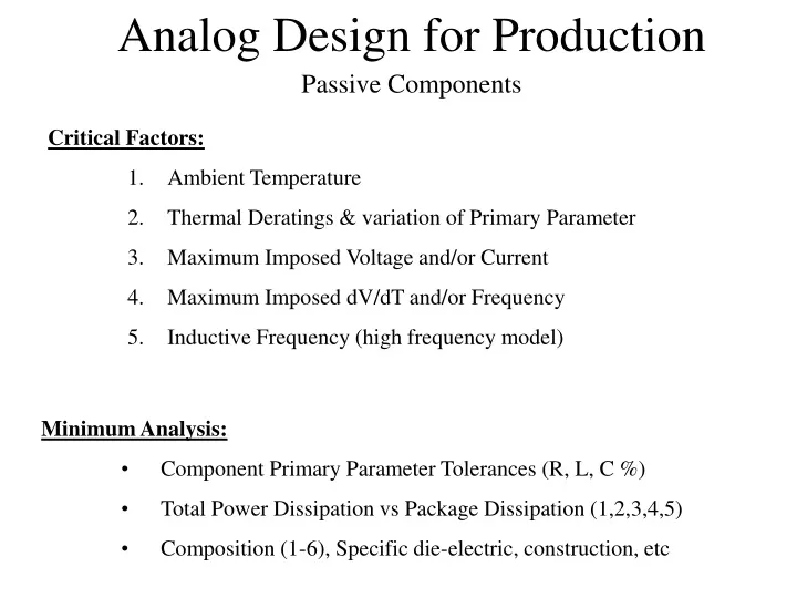
Passive Components. Critical Factors: Ambient Temperature Thermal Deratings & variation of Primary Parameter Maximum Imposed Voltage and/or Current Maximum Imposed dV/dT and/or Frequency Inductive Frequency (high frequency model). Minimum Analysis:

E N D
Passive Components • Critical Factors: • Ambient Temperature • Thermal Deratings & variation of Primary Parameter • Maximum Imposed Voltage and/or Current • Maximum Imposed dV/dT and/or Frequency • Inductive Frequency (high frequency model) • Minimum Analysis: • Component Primary Parameter Tolerances (R, L, C %) • Total Power Dissipation vs Package Dissipation (1,2,3,4,5) • Composition (1-6), Specific die-electric, construction, etc
Small Signal Amplifiers • Critical Factors: • Component Tolerances, particularly gain setting R’s • OpAmp Input Offset Voltage (Vio), worse for high gain • Input Bias Current (Ib), Input Offset Current (Iio) • Finite Diff Gain (Ad) & Variation of Ad with Frequency • Output Slew Rate and Output Vp-p at Maximum Frequency • Worst Case Analysis: • Total DC Offset error in Volts (1,2,3) • Total Gain Error vs Nominal, Converted to Volts (1,4) • Power Bandwidth for Application (1,5)
Filters • Critical Factors: • Passive Component Tolerances • OpAmp Input Offset Voltage (Vio), worse for high gain • Input Bias Current (Ib), Input Offset Current (Iio) • Loading effects of input source, output loads • Output Slew Rate and Output Vp-p at Maximum Frequency • Worst Case Analysis: • Transfer Function Analysis • Total DC Offset error in Volts (1,2,3) • Mag (dB) & Phase (deg) vs Frequency Plots (1,4) • Power Bandwidth for Application (1,5) • Pulse Response (topology, 4)
Comparators • Critical Factors: • Passive Component Tolerances, Diode Clamp Tolerances • Input Offset Voltage (Vio) • Input Bias Current (Ib), Input Offset Current (Iio) • Voh, Vol clamping voltages • Output Slew Rate and Delay • Vref Tolerance • Worst Case Analysis: • Vutp and Vltp (upper and lower trip points, 1,2,3,4,6) • Total hysteresis voltage (1-4,6) • Max switching frequency (5)
Oscillators • Critical Factors: • Passive Component Tolerances • Loading effects of output loads • Output Slew Rate and Output Vp-p at Frequency of Oscillation • Worst Case Analysis: • Transfer Function Analysis of any Linear Feedback Circuit • Forward path gain Analysis at 0 or 180 deg phase response • Mag (dB) & Phase (deg) Margins vs Frequency Plots (1,2) • Variation of Fo (1,2) • Power Bandwidth (3)
Voltage Regulators, Power Supplies • Critical Factors: • Passive Component Tolerances (voltage set resistors) • Loading effects • Input voltage DC, AC and noise levels • Filtration Capacitors • Ambient Temperature • Worst Case Analysis: • DC Output voltage variation (1,2,3) • AC Output ripple, noise (2,3,4) • Critical device power dissipation, Junction Temp (2,3,5) • Startup Output voltage vs Input voltage vs Time (2,3,4) • Safety Considerations