Download
1 / 11
110 likes | 191 Views
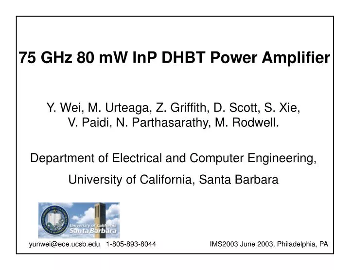
75 GHz 80 mW InP DHBT Power Amplifier. Y. Wei, M. Urteaga, Z. Griffith, D. Scott, S. Xie, V. Paidi, N. Parthasarathy, M. Rodwell. Department of Electrical and Computer Engineering, University of California, Santa Barbara.

E N D
75 GHz 80 mW InP DHBT Power Amplifier Y. Wei, M. Urteaga, Z. Griffith, D. Scott, S. Xie, V. Paidi, N. Parthasarathy, M. Rodwell. Department of Electrical and Computer Engineering, University of California, Santa Barbara yunwei@ece.ucsb.edu 1-805-893-8044 IMS2003 June 2003, Philadelphia, PA
UCSB IMS2003 W-band MMIC power Amplifiers Yun Wei • Applications for electronics in 75-110 GHz frequency band • Wideband communication systems, Atmospheric sensing, Automotive radar • 2 stage 94 GHz 0.15 m InP HEMT power amplifier: Pout= 316 mW • Y.C.Chen et. Al. IPRM, May 1999 • Cascode 78 GHz InAlAs SHBT power amplifier:Pout= 12 mW • J. Guthrie et. Al, IPRM, May 2000 • Single stage 85 GHz InP DHBT power amplifiers: Pout= 40 mW • Y. Wei et. Al, IMS, June 2002 • This work • Single stage 75 GHz HBT power amplifiers: Pout= 80 mW • Transferred substrate InP/InGaAs/InP DHBT Highest Reported Power for HBTs in W-band
M. Urteaga Transferred substrate HBT technology UCSB IMS2003 Yun Wei ε=2.7 Gains are high at 220 GHz, but fmax can’t be extrapolated
Submicron transferred-substrate HBTs and amplifier UCSB IMS2003 Yun Wei InAlAs/InGaAs TS HBTs: 0.3 m Three-stage amplifier designs: 8.5 dB gain at 195 GHz,M. Urteaga GaAs IC 2002 InP TS DHBT: AE=0.4 x 7.5 m2, AC=1.0 x 8.75 m2, JC=1.8 mA/m2, VBR,CEO = 8 V fmax = 460 GHz, ft = 139 GHz, S. Lee DRC2002
Transferred substrate power HBT and amplifier (IMS2002) UCSB IMS2003 Yun Wei 8 x ( 1 mm x 16 mm emitter )8 x ( 2 mm x 20 mm collector ) Vbr_ceo>7 V, Imax=130mA f0=85 GHz, BW3-dB=28 GHz, GT=8.5 dB P1-dB=14.5 dBm, Psat=16dBm
UCSB Thermal instability in power HBTs IMS2003 Yun Wei f1 f2 f3 f4 Ic 4-emitter-finger HBT topology Jc Multiple finger thermal instability- Current Hogging Long finger thermal instability HBT thermal stability factor
LDE doping level must not limit maximum current density LDE resistance UCSB Long emitter ballasting: Lightly doped emitter expitaxy IMS2003 Yun Wei Ti/Pt/Au emitter contact InGaAs 1x10¹⁹, 300 Å emitter cap InGaAs/InAlAs 2x10¹⁹, 90 Å grade InP 5x10¹⁶, 1000 Å LDE emitter Band profile Bias at Vbe=0.7 V, Vce=1.5 V InP 8x10¹⁷, 300 Å emitter * un=2000cm2/V.S
UCSB 1/4 Amp, 220 GHz fmaxInP Power DHBT IMS2003 Yun Wei 8 x ( 1 mm x 24 mm emitter )8 x ( 2 mm x 28 mm collector )~8 Ohm ballast per emitter finger fmax>230 GHz VBR_CE>7 V Imax=250mA 192 mm2 common base LDE DHBT IE step=50 mA Optimum load bias condition Ic=140 mA, Vce=3.7 V
UCSB Amplifier Design IMS2003 Yun Wei • Common-base, optimum load match • 8dB gain, 21 dBm output power • self-developed multi-finger large signal HBT model with thermal effects • electromagnetic simulation of all passive elements (Agilent Momentum)
UCSB IMS2003 Amplifier Measurements Yun Wei Small signal measurement • f0=75 GHz, GT=5.6 dB • P1-dB=18 dBm, Psat=19 dBm @ 4dB gain • Device dimensions: • Emitter area: 1x16x16=256 m2 • Collector area: 2x20x16=640 m2 • Device bias conditions: • Ic=130 mA, Vce=4.5 V Large signal measurement Die size: 0.38 mm 0.89 mm
UCSB Conclusions IMS2003 Yun Wei • Demonstrated Wideband Power DHBT: Ic_max> 240 mA, Vce_BR>7 V, fmax=300 GHz • Wideband Power amplifiers: f0=75 GHz, GT=5.6 dB, Psat=19dBm • Multi-finger emitter ballasting scheme provides direction for future high power and high frequency MMIC work in transferred-substrate process • Future work • Multi-stage wideband high power amplifiers • ~200 GHz power amplifiers • Acknowledgements • This work is funded by ARO-MURI program under contract number PC249806.