Download
1 / 27
340 likes | 795 Views
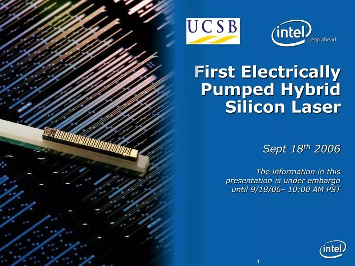
First Electrically Pumped Hybrid Silicon Laser . Sept 18 th 2006 The information in this presentation is under embargo until 9/18/06– 10:00 AM PST. Agenda. Dr. Mario Paniccia Director, Photonics Technology Lab Dr. John Bowers Professor, UC Santa Barbara What We are Announcing

E N D
First Electrically Pumped Hybrid Silicon Laser Sept 18th 2006The information in this presentation is under embargo until 9/18/06– 10:00 AM PST
Agenda Dr. Mario Paniccia Director, Photonics Technology Lab Dr. John Bowers Professor, UC Santa Barbara • What We are Announcing • Silicon Photonics Overview • Lasers & Light Emission with Silicon Photonics • Joint Collaboration – Hybrid Silicon Laser • Hybrid Silicon Laser Test Results • Summary
What We are Announcing • Research Breakthrough: 1st Electrically pumped Hybrid Silicon Laser • A joint collaboration between UCSB and Intel Corporation • Combines the light emitting capabilities of Indium phosphide with the high volume, low cost capabilities of silicon • Addresses one of the last major hurdles to silicon photonic chips • Vision: • Build chips containing 10 to hundreds of Hybrid Silicon Lasers • Built using high-volume, low cost manufacturing processes • Enables terabit optical links • Background • Silicon is a poor light emitter while Indium phosphide based materials are great light emitters • However, Indium phosphide lasers are expensive to manufacture • Novel design combined with a manufacturing process where a unique “glass glue” was used to bond the two materials together
The Photonic Dilemna • Fiber can carry much more bandwidth than copper • However, it is much more expensive…..
Optical Copper Chip to Chip1 – 50 cm Metro & Long Haul Billions 0.1 – 80 km Board to Board50 – 100 cm Volumes Millions Rack to Rack 1 to 100 m Thousands Today's High Speed Interconnects Decreasing Distances Goal: Drive optical to high volumes and low costs
Photonics: The technology of emission, transmission, control and detection of light (photons) aka fiber-optics & opto-electronics Today: Most photonic devices made with exotic materials, expensive processing, complex packaging Silicon Photonics Vision: Research effort to develop photonic devices using silicon as base material and do this using standard, high volume silicon manufacturing techniques in existing fabs Benefit: Bring volume economics to optical communications
Continuous Wave Silicon Raman Laser(Feb ‘05) 1GHz ( Feb ‘04)10 Gb/s (Apr ‘05) Intel’s Silicon Photonics Research Electrically Pumped Hybrid Silicon laser (September 2006) First: Innovate to prove silicon is a viable optical material
TODAY Device level – Prove silicon viable FUTURE Monolithic? Integrate silicon devices into hybrid modules Integration Vision Time Increasing silicon integration over time
FLASH BULB LASERBEAM RUBY CRYSTAL ROD The First Laser Developed by Maiman, this ruby laser used a flash bulb as an optical pump Fully ReflectiveMirror Partially Reflective Mirror Published in Nature, August 6, 1960
Radiative recombination coefficient (10-12cm3/s) First CW silicon laser • Research Breakthrough • Based on the Raman effect • Optically pumped Stimulated Emission Want: Electrically Pumped • Silicon is an indirect bandgap material • Poor radiative recombination coefficient • Result: Silicon emits heat, few photons Indium Phosphide Gallium Arsenide Indium Antimonide Germanium Silicon Raman Laser Announced in Feb 2005
Options for Integrating Light Sources Hybrid Silicon Laser • Bond InP based material to Silicon • No alignment • Many lasers with one bonding step • Amenable to high integration • Potentially lowest cost Off-chip Laser • High power laser required • Requires fiber attach • Non-integrated solution • Expensive Direct Attached Laser • Tight alignment tolerances • Requires gold metal bonding • Passive alignment challenges • Less Expensive
Joint Intel / UCSB Collaboration • Goal: Create a hybrid silicon laser • Combine the light emitting properties of Indium phosphide with light routing and manufacturability properties of silicon Joint team and 3 year research grant UCSB – Indium phosphide and wafer bonding expertise • Alex Fang (ex Intel intern) • Professor John Bowers • Hyundai Park Intel – Silicon and manufacturing expertise • Dr Richard Jones • Oded Cohen • Dr Mario Paniccia
Hybrid Silicon LaserUsing Evanescent Coupling • We start with a cross sectional view of an Indium Phosphide waveguide Indium Phosphide waveguide Cross Section • When a voltage is applied to the InP it will begin to emit light • If we bring a silicon waveguide up to the InP, light will couple into the Si waveguide • This is evanescent coupling Challenge: How do you bond these two materials together?
Bonding Process The Hybrid Silicon Laser used a unique bonding technique • Previous attempts used crystal growth • Difficult to overcome lattice mismatch/threading dislocation • Causes poor performance • Benefits of the UCSB/Intel approach • Removes issue with lattice mismatch • Plasma process produces ~25 atom thick “glass-glue” • This “glass-glue” efficiently bonds the two materials • Low temperature manufacturable process Indium Phosphide Silicon
Process Animation 1) A waveguide is etched in silicon 2) The Indium phosphide is processed to make it a good light emitter 3) Both materials are exposed to the oxygen plasma to form the “glass-glue” 4) The two materials are bonded together under low heat
Process Animation 5) The Indium phosphide is etched and electrical contacts are added 6) Photons are emitted from the Indium Phosphide when a voltage is applied 7) The light is coupled into the silicon waveguide which forms the laser cavity. Laser light emanates from the device.
Hybrid Silicon LaserHow we create a laser in silicon • The Indium Phosphide emits the light into the silicon waveguide • The silicon acts as laser cavity: • Silicon waveguide routes the light • End Facets are reflectors/mirrors • Light bounces back and forth and get amplified by InP based material
Hybrid Laser Structure SEM (Scanning Electron Microscope) Photograph
First Electrically Pumped CW Lasing Measured Laser output power vs current • Threshold Current • At 65 mA with plans to get to ~ 20 mA • Output power • At 1.8 mW, Good for optical interconnects • Temperature • Operating at 40 C with plans for > 70 C Threshold Voltage = 2V Initial testing shows good performance
Electrically Pumped Laser Wavelength • 7 Hybrid Silicon Lasers • All fabricated with a single bond step • Up to 36 lasers are on one die • Lasing Output at 1577nm • This is adjustable via modifying the silicon waveguides
1 inch Silicon Hybrid Laser
Era ofTera-ScaleComputing 10’s to 100’sof cores Quad-Core More performance Using less energy Dual Core Hyper-Threading The days ofsingle-core chips Instruction level parallelism TIME Tera-leap to Parallelism: ENERGY-EFFICIENT PERFORMANCE All this compute capability may require high speed optical links
High Integration Optical Fiber Multiplexor 25 modulators at 40Gb/s 25 hybrid lasers An future integrated terabit per second optical link on single chip
Integrating into a Tera-scale System This transmitter would be combined with a receiver Rx Tx Which could then be built into an integrated, silicon photonic chip!!
Integrating into a Tera-scale System This integrated silicon photonic chip could then be integrated into computer boards And this board could be integrated into a Tera-scale system
Summary • Research Breakthrough: 1st Electrically pumped Hybrid Silicon Laser • A joint collaboration between UCSB and Intel Corporation • Combines the light emitting capabilities of Indium phosphide with the high volume, low cost capabilities of silicon • Addresses one of the last major hurdle to silicon photonic chips • Vision: • Build chips containing 10 to 100s of Hybrid Silicon Lasers • Built using high-volume, low cost manufacturing processes • Enables terabit optical links • Background • Silicon is a poor light emitter while Indium phosphide based materials are great light emitters • However, Indium phosphide lasers are expensive to manufacture • Novel design combined with a manufacturing process where a unique “glass glue” was used to bond the two materials together
Acknowledgements: UCSB and Professor Bowers would like to thank Jag Shah and DARPA for funding some of this research.