Download
1 / 85
860 likes | 1.49k Views
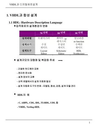
1. VHDL 과 합성 설계 1.1 HDL: Hardware Description Language 집적회로의 설계환경의 변화 설계규모의 대형화 및 복잡화 추세 - 간결한 하드웨어 표현 - 편리한 문서화 - 설계 정보의 교환 - 상위 레벨에서의 설계 자동화 필요 - 설계 자동화 도구의 변화 : 모델링 , 합성 , 검증 , 설계 모듈 관리 HDL 의 예 - C, AHPL, CDL, IDL, TI-HDL, UDL 등 - VHDL, Verilog-HDL.

E N D
1. VHDL과 합성 설계 1.1 HDL: Hardware Description Language 집적회로의 설계환경의 변화 설계규모의 대형화 및 복잡화 추세 - 간결한 하드웨어 표현 - 편리한 문서화 - 설계 정보의 교환 - 상위 레벨에서의 설계 자동화 필요 - 설계 자동화 도구의 변화 : 모델링, 합성, 검증, 설계 모듈 관리 HDL의 예 - C, AHPL, CDL, IDL, TI-HDL, UDL 등 - VHDL, Verilog-HDL
1.2 VHDL의 등장과 특징 VHDL(VHSIC HDL)의 출현 - 1981년 6월 미국 Woods Hole에서 개최된 하드웨어 기술언어 Workshop에서 미국방성의 VHSIC(Very High Speed Integrated Circuit) 프로그램에서 요구되는 HDL사양을 근간으로 하는 미국방성의 HDL 요건(Department of Defense Requirements for HDL)이라는 공식 문건을 발간 VHDL개발의 근간 - 1983년 7월 Intermetrics, IBM, Texas Instruments 사로 구성된 공동 개발팀 구성 - 1985년 VHDL 7.2 Version 탄생 초기개발 목적을 설계의 문서화와 시뮬레이션에 둠 - 1987년 12월 IEEE 1076 표준 탄생 미국방성과의 계약 체결 뿐만 아니라 산업체에서의 상업용으로 사용할 수 있도록 확장 - 1991년 IEEE 1076에 추가적으로 합성기능의 강화 관련 CAD 업체의 본격적인 합성 도구 개발이 시작 - 1992년 미 정부지원 공인 HDL로 VHDL을 지정 - 1993년 VHDL응용과정에서의 추가요건을 반영한 IEEE 1076-1993 - 국내외적으로 VHDL의 사용이 확대되고 있으며 VHDL 시뮬레이터 및 합성을 대부분의 설계자동화 도구에서 지원
VHDL을 이용한 설계의 특징 - 설계 싸이클의 단축 : 초기 설계과정에서의 설계 오류 수정 합성 설계에 의한 도면 생성 및 관리 작업의 불필요 설계 변경의 용이 - 설계의 질 향상 : 다양한 설계기법의 검색에 의한 최적해 도달 선택적 최적화 기법을 이용한 합성 설계 - Technology에 무관한 description 및 설계 : 특정 ASIC 제조업체 및 특정 구현 기술과 무관하게 초기 설계 및 기술 가능 ( 설계 싸이클의 마지막에 고려) 동일한 VHDL 설계의 다른 라이브러리를 이용한 합성 신속한 칩 원형화 (rapid prototyping) 가능 - 낮은 설계 비용 : 상위레벨 설계 도구의 사용에 따른 설계 생산성 향상 설계 기간 단축에 따른 설계 비용 감소 설계의 재사용에 의한 설계 비용의 감소
- 표준 HDL 및 사용의 확대 : IEEE 표준인 동시에 미국 정부의 공인 HDL 전세계적으로 설계 및 설계정보 교환의 수단으로 사용이 점차적으로 확대 - 기술에 따른 성장 : 반도체 기술 및 ASIC 기술 발전에 따른 VHDL 합성설계 도구의 기능 및 능력의 확장 - 효과적인 설계관리 : VHDL 언어의 structured design 기능을 이용한 전체 설계의 기능별 분할 설계 및 설계의 관리 및 문서화 용이 IC제조 기술 발전 ASIC (Application Specific IC) 등장 설계 도구 성능 향상 -주문형( semi-custom )반도체 -소량 ( application specific ) -개발 기간 단축 ( shorter design turnaround time (DAT))
1.3 VHDL과 ASIC 설계 환경 가. 합성 가능한 함수 및 합성 원칙 합성 가능한 함수 - ASIC설계를 사용한 디지털 시스템은 일반적으로 랜덤 로직, 메모리, 그리고 megafunction 등으로 이루어짐 - 랜덤 로직 회로 설계는 게이트나 플립플롭과 같은 primitive logic cell을 building block으로 하여 논리합성함이 효율적이다 - RAM이나 ROM과 같은 규칙적인 구조의 메모리의 설계는 일반적으로 전용 컴파일러를 사용함이 적절하다 - 합성 가능한 조합형 논리 함수 예: Multiplexer, Decoder, Encoder, Comparator, Adder/Subtractor, ALU, Multiplier, Lookup table, Parity generator, PLA, Gates 등 - 합성 가능한 순차형 논리 함수 예: 각종 Counter, Register, Latch, Parallel/Serial converter, Sequencer, Controller, Finite state machine, Synchronizer 등
언어로 기술할 경우 회로 복잡도에 상관없음. 회로가 점차 복잡해짐 잦은 설계 변경 용이. 성능 평가 netlist 자동 추출. DAT 단축 circuit design with HDL VHDL 합성의 필요성 logic synthesis 초기 설계 단계에서 오류 검출 simulation
VHDL 합성에서의 유의사항 - VHDL 합성설계 방식은 VHDL로 설계를 기술하고 시뮬레이션하며 이 VHDL 모델을 합성시스템을 이용하여 논리회로로 변환하는 설계 방식이다 1) 합성회로의 결과는 VHDL 표현방식에 따라 크게 좌우된다. 즉, VHDL 기술방식에 따라 합성된 결과 회로는 기능은 동일하더라도 게이트의 수 또는 critical path, 그리고 회로의 구조 등이 다를 수 있다 자신이 원하는 논리구조로 합성해 낼 수 있도록 VHDL 코딩 할 수 있어야 한다. 2) 시뮬레이션 가능한 모든 VHDL code 모두 합성 가능한 것은 아니다. 일반적으로 합성 가능한 code는 RTL(Register Transfer Level) 기술로 하여야 하며 tool dependent 하다. 3) 합성 설계를 성공적으로 수행하기 위해서는 논리회로 설계 기법에 익숙하고 ASIC 설계 경험 또한 풍부하여야 한다 4) VHDL test bench를 이용하여 합성 전후의 효과적인 시뮬레이션을 수행함이 바람직하다
System Design & Partitioning 기본적인 시스템 요건 분석 적용 가능한 알고리즘의 분석 하드웨어, 소프트웨어 설계 분할 ASIC의 설계 사양 및 블록도 ASIC의 논리함수 구현 방법 시스템 인터페이스 방식 등 ASIC Block Diagram & Specification 나. ASIC 설계 프로세스 VHDL 모델링, RTL 시뮬레이션 설계의 수정 및 설계최적화 Technology Targeting & Synthesis Logic Design Logic Simulation 게이트 레벨 시뮬레이션 Layout 및 배선 타이밍분석, 설계규칙 검사 전기규칙검사 및 I/O 핀 할당 Pre and Post-Layout Verification Prototype ASIC Fabrication & Test
Schematic Entry VHDL Coding 다. 논리회로 설계 흐름도의 비교 Netlist Generation RTL Level VHDL Simulation Gate Level Logic Simulation Logic Synthesis A) 기존의 게이트 레벨 논리회로 B) VHDL 합성을 이용한 논리회로 설계 흐름도 설계 흐름도
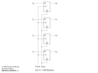
VHDL 합성설계 2. VHDL 합성설계의 기본과 Coding Issues 2.1 4가지 VHDL code 예 - D flip flop, Latch, AND 게이트, Multiplexer의 예를 통하여 비슷한 VHDL 기술 스타일과 원하는 합성 회로의 차이를 유의하여야 한다. 가. D Flip Flop entity D_FF is port( b, c : in bit; qout : out bit); end D_FF; architecture test of D_FF is begin process begin waituntil clk’event and clk = ‘1’; qout <= b; end process; end test; b D Q clk qout c
나. Latch entity D_Latch is port(data, enable : in bit; qout : out bit); end D_Latch; architecture test of D_Latch is begin process(data, enable) begin if (enable = ‘1’) then qout <= data; end if; end process; end test; data D Q Enable qout enable
다. 2-입력 AND 게이트 entity AND2 is port( b, c : in bit; and_out : out bit); end AND2; architecture test of AND2 is begin process begin if (c = ‘1’) then and_out <= b; else and_out <= ‘0’; end if; end process; end test; b and_out c
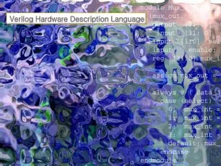
라. 2 x 1 Multiplexer entity MUX is port( b, c, s : in bit; mux_out : out bit); end MUX; architecture test of MUX is begin process begin case s is when ‘0’ <= mux_out <= b; when ‘1’ <= mux_out <= c; endcase; end process; end test; b 0 1 select mux_out c s 주의 : 위와 같이 s의 값이 ‘1’이 아닐 때 출력의 값이 분명히 명시가 되어 있으면 멀티플렉서가 합성되지만 그렇지 않을 경우 출력은 이전 값을 유지하는 latch가 합성된다
2.2 일반적인 VHDL Coding Issues 가. VHDL Types - 설계 hierarchy 상에서 서로 다른 레벨에서 합성된 netlist를 통합하고 자 할 때 변환함수(conversion function)의 사용을 피하기 위해서는 entity 에서의 port 선언을 위해서 std_logic자료형(type)을 사용하는 것이 좋다. - 자료형의 일관성을 유지하기 위하여 자료형 ‘buffer’의 사용을 피하 는 것이 좋다. 아래의 예는 내부 signal을 이용하여 자료형 ‘buffer’의 사용을 피하는 효과적인 방법을 보여 준다. entity buf is port ( a, b : in std_logic ; c : out std_logic ); end buf ; architecture Behavioral of buf is signal c_int : std_logic ; begin process begin c_int <= a + b + c_int ; end process c <= c_int ; end Behavioral;
나. Signals and Variables - 시뮬레이션시 Signal은 값이 update 될 때 delta time이 있지만 Variable은 delay 없이 즉시 값이 바뀐다. - Variable을 사용시 시뮬레이션은 빨라지지만 설계의 기능성에 영향을 미칠 수 있는 glitch의 검출을 놓칠 수 있다. - Variable은 시뮬레이션 중 예상치 않은 결과를 발생시킬 가능성이 높다 다. Priority Encoding Structure - 통상 ‘if’ 문의 조건문 순위는 회로 합성시 priority encoding 회로로 추론 된다. 따라서, 이를 피하기 위해서는 ‘case’ 문을 사용하여야 한다. VHDL 예제 : 두개의 load signal을 갖는 8-비트 카운터를 모델링하고자 한다. Signal ‘load0’가 active 일 때 bus의 하위 4비트가 카운터의 하위 4비트로 load 되고, signal ‘load1’이 active 일 때 bus의 상위 4비트가 카운터의 상위 4비트로 load 되며, 그 이외의 경우는 카운터가 가산을 한다. load1 load0 MSB LSB 8-비트 카운터 8-비트 BUS
Library IEEE use IEEE.std_logic_1164.all ; use IEEE.std_logic_unsigned.all ; entity ld_cnt is port ( load : in std_logic_vector(1 downto 0) ; databus : in std_logic_vector(7 downto 0) ; clk : in std_logic ; count : out std_logic_vector(7 downto 0) ; end ld_cnt ; architecture behavior of ld_cnt is signal int_cnt : std_logic_vector(7 downto 0) ; begin count <= int_cnt ; process begin waituntil clk=‘1’ and clk’event ; if(load = “10”) then int_cnt <= databus(7 downto 4) & int_cnt(3 downto 0) ; elsif (load = “01”) then int_cnt <= int_cnt(7 downto 4) & databus(3 downto 0) ; else int_cnt <= int_cnt + 1 ; end if ; end process ; end behavior;
라. 원치 않는 Latches - 원치 않는 Latch가 합성되지 않게 하기 위해서는 ‘if’ 문과 ‘case’ 문의 기술시 모든 조건을 빠짐없이 포함시켜야 한다(2.1 참조) 마. 동기식과 비동기식 Resets - 동기식 reset 신호를 갖는 회로는 ‘if’ 문이 클록문(clock statement) 이 후에 나타나야 하며, 비동기식 reset 신호를 갖는 회로는 ‘if’ 문이 클 록문 이전에 나타나야 한다. 비동기 reset 신호를 갖는 설계의 예: entity test_reset is port ( X, clk, rst : in bit ; Z : out bit ) ; end test_reset ; architecture behavior of test_reset is type state is (S0, S1, S2, S3); signal ST: state; begin
process begin if rst = ‘0’ then ST <= S0 ; Z <= ‘0’ ; elsif clk’event and clk = ‘1’ then if X = ‘0’ then Z <= ‘0’ ; else case ST is - - - endcase ; endif ; end process ; end behavior ; 동기 reset 신호를 갖는 설계 : architecture behavior of test_reset is begin waituntil clk’event and clk = ‘1’ ; if rst = ‘0’ then ST <= S0 ; Z <= ‘0’ ; elsif X = ‘0’ then Z <= ‘0’ ; else case ST is -- 이후의 기술은 비동기식에서의 예와 같음 --
3. 기본 논리회로의 설계 예 - 3장에서의 기본 논리회로의 VHDL 합성설계의 예는 주로 LODECAP 에서의 Sample 들과 기타 기본 회로들로 구성하였다. 3.1 조합회로의 예 가. Multiplexer Ô 2-way 2 x 1 multiplexer : <muxType1.vhd> library IEEE; use IEEE.std_logic_logic_1164.all; use IEEE.std_logic_signed.all; entity muxType1 is port(a, b : IN std_logic_vector(1 downto 0); s : IN std_logic; z : OUT std_logic_vector(1 downto 0)); end muxType1; architecture RTL of muxType1 is signal TMP : std_logic_vector(1 downto 0); begin z <= a when s = ‘0’ else b; end RTL; a 2 2 2 x 1 MUX z b 2 s
Ô 2-way 2 x 1 multiplexer : <muxType2.vhd> library IEEE; use IEEE.std_logic_signed.all; use IEEE.std_logic_signed.all; entity muxType2 is port(a, b : IN std_logic_vector(1 downto 0); s : IN std_logic; z : OUT std_logic_vector(1 downto 0)); end muxType2; architecture RTL of muxType2 is signal TMP : std_logic_vector(1 downto 0); begin process(a, b, s) begin if s = ‘0’ then z <= a; else z <= b; endif; endprocess; end RTL; 4 x 1 MUX 2 a z 2 2 b s
4 x 1 MUX 2 a z 2 2 b 2 c 2 d 2 s(1:0) Ô 2-way 4 x 1 multiplexer : <muxType3.vhd> library IEEE; use IEEE.std_logic_1164.all; use IEEE.std_logic_signed.all; entity muxType3 is port(a, b, c, d : IN std_logic_vector(1 downto 0); s : IN std_logic(1 downto 0); z : OUT std_logic_vector(1 downto 0)); end muxType3; architecture RTL of muxType3 is begin process(a, b, c, d, s) begin case s is when “00” => z <=a; when “01” => z <=b; when “10” => z <=c; when “11” => z <=d; whenothers => z <=“00”; endcase; endprocess; end RTL;
4 x 1 MUX 4 I0 Y 4 I1 4 I2 4 I3 2 SEL(1:0) Ô Enable 갖는 4-way 4 x 1 multiplexer : <mux4.vhd> library IEEE; use IEEE.std_logic_1164.all; use IEEE.std_logic_signed.all; entity MUX4 is port(l0, l1, l2, l3 : IN std_logic_vector(3 downto 0); ENABLE : IN std_logic; SEL : IN std_logic_vector(1 downto 0); Y : OUT std_logic_vector(3 downto 0)); end MUX4; architecture RTL of MUX4 is begin process ( SEL, ENABLE, l0, l1, l2, l3) begin if ENABLE = ‘0’ then case SEL is when “00” => Y <= l0; when “01” => Y <= l1; when “10” => Y <= l2; whenothers=> Y <= l3; endcase; else Y <= “0000”; elseif; endprocess; end RTL; ENABLE
나. Decoder 회로 Ô 2-to-4 decoder <decoder1.vhd> library IEEE; use IEEE.std_logic_1164.all; use IEEE.std_logic_signed.all; entity decoder1 is port(a : IN std_logic_vector(1 downto 0); d : OUT std_logic_vector(3 downto 0)); end decoder1; architecture RTL of decoder1 is begin process begin case a is when “00” => d <= “0001”; when “01” => d <= “0010”; when “10” => d <= “0100”; whenothers => d <= “1000”; endcase; endprocess; end RTL; decoder1 2 4 a d
그림 7. Decoder1의 합성 회로 그림 8. Decoder1의 시뮬레이션 결과
Ô BCD-to-7segment decoder <BCD_7.vhd> y(6) BCD-to-7 Segment Decoder G G y(5) F y(4) F B E 4 y(3) A D y(2) BCD_data C E C y(1) B D y(0) A library IEEE; use IEEE.std_logic_1164.all; entity BCD_7 is port(BCD_data : IN std_logic_vector(3 downto 0); Y : OUT std_logic_vector(6 downto 0)); end BCD_7;
architecture RTL of BCD_7 is begin process(BCD_data) begin case BCD_data is when “0000” => Y <= “1111110”; when “0001” => Y <= “0110000”; when “0010” => Y <= “1101101”; when “0011” => Y <= “1111001”; when “0100” => Y <= “0110011”; when “0101” => Y <= “1011011”; when “0110” => Y <= “1011111”; when “0111” => Y <= “1110000”; when “1000” => Y <= “1111111”; when “1001” => Y <= “1110011”; whenothers => Y <= “0000000”; end case; end process; end RTL;
그림 9. BCD_7의 합성 회로 그림 10. BCD_7의 시뮬레이션 결과
다. Encoder 회로 Ô <encoder.vhd> 예제 library IEEE; use IEEE.std_logic_1164.all; use IEEE.std_logic_signed.all; entity encoder is port(a : IN std_logic_vector(3 downto 0); z : OUT std_logic_vector(1 downto 0)); end encoder; architecture RTL of encoder is begin z <= “00” when a(0) = ‘1’ else “01” when a(1) = ‘1’ else “10” when a(2) = ‘1’ else “11”; end RTL; encoder a(3) z(1) a(2) z(0) a(1) a(0)
Ô <func2.vhd> 예제 library IEEE; use IEEE.std_logic_1164.all; use IEEE.std_logic_signed.all; entity FUNC2 is port(A, B, C, D : IN std_logic; ENC_OUT : OUT std_logic_vector(1 downto 0)); end FUNC2; architecture RTL of FUNC2 is begin process(A, B, C, D) begin if D = ‘0’ then ENC_OUT <= “00”; elsif C = ‘0’ then ENC_OUT <= “01”; elsif B = ‘0’ then ENC_OUT <= “10”; elsif A = ‘0’ then ENC_OUT <= “11”; elsif ENC_OUT <= “00”; end if; end process; end RTL;
Ô 1-bit Full-Adder :<FA1.vhd> 예제 library IEEE; use IEEE.std_logic_1164.all; use IEEE.std_logic_signed.all; entity FA1 is port( A, B, CIN : IN std_logic; SUM,COUT : OUT std_logic); end FA1; architecture RTL of FA1 is begin process(A, B, CIN) variable TEMP : std_logic_vector(2 downto 0); begin TEMP := A & B & CIN; case TEMP is when “000” => SUM <= ‘0’; COUT <= ‘0’; when “001” | “010” | “100” => SUM <= ‘1’; COUT <= ‘0’; when “011” | “101” | “110” => SUM <= ‘0’; COUT <= ‘1’; when “111” => sum <= ‘1’; COUT <= ‘1’; when others => SUM <= ‘0’; COUT <=‘0’; end case; end process; end RTL;
Ô 9 bit adder : <adder9.vhd> library IEEE; use IEEE.std_logic_1164.all; entity adder9 is port(cin : IN std_logic; a, b : IN std_logic_vector(8 downto 0); sum : OUT std_logic_vector(8 downto 0); cout : OUT std_logic); end adder9; architecture RTL of adder9 is begin process ( cin, a, b) variable carry : std_logic; begin carry := cin; for i in 0 to 8 loop sum(i) <= a(i) XOR b(i) XOR carry; carry := (carry and (a(i) XOR b(i))) or (a(i) and b(i)); endloop; cout <= carry; end process; end RTL;
Ô Pipelined adder 회로 : < pipeAdder.vhd> library IEEE; use IEEE.std_logic_1164.all; use IEEE.std_logic_signed.all; entity pipeAdder is port ( clk : in std_logic; inBus :in std_logic_vector(7 downto 0); outBus :out std_logic_vector(8 downto 0)); end pipeAdder; architecture RTL of pipeAdder is signal reg_a : std_logic_vector(7 downto 0); signal reg_b : std_logic_vector(8 downto 0); begin outBus <= reg_b; process ( clk) begin if ( clk = ‘1’ and clk’event) then reg_a <= inBus; reg_b <= (‘0’ & reg_a) + (‘0’ & inBus); endif; endprocess; end RTL; inBus Reg_a + Reg_b Out_Bus
Ô 4-bit 수 차의 절대값 연산 : < absdiff.vhd> library IEEE; use IEEE.std_logic_1164.all; use IEEE.std_logic_signed.all; entity absdiff is port (a : IN std_logic_vector(3 downto 0); b : IN std_logic_vector(3 downto 0); d :OUT std_logic_vector(3 downto 0)); end absdiff; architecture RTL of absdiff is begin process (a, b) begin if (a > b) then d <= a - b; else d <= b - a; end if; end process; end RTL;
Ô ALU 연산 : <ALU.vhd> OP1 OP2 8 8 3 OPCODE ALU 8 ALU_OUT library IEEE; use IEEE.std_logic_1164.all; use IEEE.std_logic_signed.all; entity ALU is port(OPCODE : IN std_logic_vector(2 downto 0); OP1,OP2 : IN std_logic_vector(7 downto 0); ALU_OUT : OUT std_logic_vector(7 downto 0)); end ALU;
architecture RTL of ALU is begin process (OPCODE, OP1, OP2) begin case OPCODE is when “000” => ALU_OUT <= OP1 + OP2; when “001” => ALU_OUT <= OP1 - 1; when “010” => ALU_OUT <= OP1 - OP2; when “011” => ALU_OUT <= OP1 + 1; when “100” => ALU_OUT <= OP1 and OP2; when “101” => ALU_OUT <= OP1 or OP2; when “101” => ALU_OUT <= not OP2; whenothers => ALU_OUT <= OP1; end case; end process; end RTL;
ÔIncrement회로 : < inc.vhd> library IEEE; use IEEE.std_logic_1164.all; use IEEE.std_logic_signed.all; entity INC is port(PC_ADDR : IN std_logic_vector(4 downto 0); INC_ADDR : OUT std_logic_vector(4 downto 0)); end INC; architecture RTL of INC is begin INC_ADDR <= PC_ADDR + 1; end RTL;
Ô Decrement 회로 : <dec.vhd> library IEEE; use IEEE.std_logic_1164.all; use IEEE.std_logic_signed.all; entity DEC is port(PC_ADDR : IN std_logic_vector(4 downto 0); DEC_ADDR : OUT std_logic_vector(4 downto 0)); end DEC; architecture RTL of DEC is begin DEC_ADDR <= PC_ADDR -1; end RTL;
3.2 순차회로의 예 가. 계수기(counter) Ô 6-bit up counter 회로 : < upCount.vhd> library IEEE; use IEEE.std_logic_1164.all; use IEEE.std_logic_signed.all; entity upCount is port(CLK32M, MRESET : in std_logic; upCountOut : out std_logic_vector(5 downto 0)); end upCount; architecture RTL of upCount is signal TMP : std_logic_vector(5 downto 0); begin upCountOut <= TMP; process (CLK32M, MRESET) begin if MRESET = ‘1’ then TMP <= “000000”; elsif (CLK32M = ‘0’ and CLK32M’event) then TMP <= TMP + ‘1’; end if; endprocess; end RTL;
Ô Enable과 load가 있는 6-bit up-counter 회로 : <upCount2.vhd> library IEEE; use IEEE.std_logic_1164.all; use IEEE.std_logic_signed.all; entity upCount2 is port( clk, reset, enable, load : in std_logic; dataBus : in std_logic_vector(5 downto 0); upCount2Out : out std_logic_vector(5 downto 0)); end upCount2; architecture RTL of upCount2 is signal TMP : std_logic_vector(5 downto 0); signal clkEnable : std_logic; begin upCount2Out <= TMP; clkEnable <= clk and enable; process ( clkEnable, reset, load) begin if reset ‘1’ then TMP <= “000000”; elsif ( clkEnable = ‘1’ and clkEnable’event) then if load = ‘1’ then TMP <= dataBus; else TMP <= TMP + ‘1’; endif; end if; end process; end RTL;