Download
1 / 5
50 likes | 219 Views
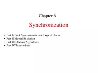
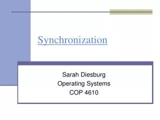
TX_EN TX_ER TXD. MPC TLK2501 TRNS. SP TLK2501 RCVR. RX_DV RX_ER RXD. MPC–SP Synchronization. Problems: Receiver to Transmitter Serial Clock Synchronization 32 bit @ 40 MHz from 2 x 16 bit @ 80 MHz Frames Recovery Options: Using TLK2501 Transmit Control / Receive Status bits ( 1,2 )

E N D
TX_ENTX_ERTXD MPCTLK2501TRNS SPTLK2501RCVR RX_DVRX_ERRXD MPC–SP Synchronization • Problems: • Receiver to Transmitter Serial Clock Synchronization • 32 bit @ 40 MHz from 2 x 16 bit @ 80 MHz Frames Recovery • Options: • Using TLK2501 Transmit Control / Receive Status bits (1,2) • Using a Frame Bit in the Data Format (2) LINK Lev Uvarov
Frame Bit Option NO room for a Frame bit Lev Uvarov
TLK2501 Control / Status Option Table 1. Transmit Data Controls Table 2. Receive Status Signals 2-bit TLK2501 Control / Status allows proper synchronization Lev Uvarov
GTX_CLK TX_EN TX_ER RX_CLK RX_DV RX_ER TXDn BC3563:FR0 BC3563:FR1 BC0:FR1 BC0:FR2 RXDn IDLE IDLE BC0:FR1 BC0:FR2 Transmit / Receive Timing Figure 1. Transmit Side Timing Diagram Figure 2. Receive Side Timing Diagram Lev Uvarov
TLK2501 RECEIVERS RX_DVRX_CLKRXD ENW ENRWCLK RCLK WDATA RDATA 1 RX_DVRX_CLKRXD ENW ENRWCLK RCLK WDATA RDATA 2 RX_DVRX_CLKRXD ENW ENRWCLK RCLK WDATA RDATA 15 & DQCLK RD_CLK BX Synchronization ALIGNMENT FIFOs BC0 : FR1 Figure 3. Simplified Alignment Schematics. Each channel enables FIFO writes as soon as its RX_DV becomes HIGH (i.e. on bunch crossing Zero, First Frame). The latest channel enables FIFO reads. All FIFOs read BC0 : FR1 as a first word. Lev Uvarov