Download
1 / 14
150 likes | 319 Views
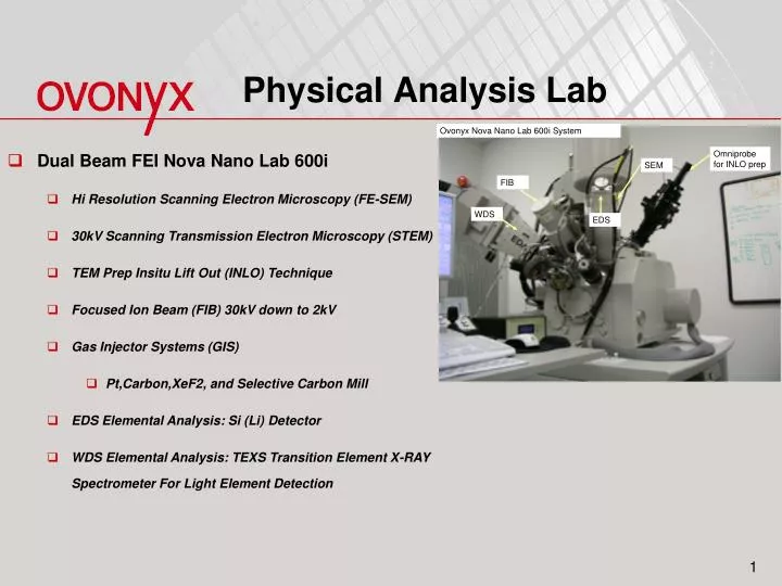
Physical Analysis Lab. Dual Beam FEI Nova Nano Lab 600i Hi Resolution Scanning Electron Microscopy (FE-SEM) 30kV Scanning Transmission Electron Microscopy (STEM) TEM Prep Insitu Lift Out (INLO) Technique Focused Ion Beam (FIB) 30kV down to 2kV Gas Injector Systems (GIS)

E N D
Physical Analysis Lab • Dual Beam FEI Nova Nano Lab 600i • Hi Resolution Scanning Electron Microscopy (FE-SEM) • 30kV Scanning Transmission Electron Microscopy (STEM) • TEM Prep Insitu Lift Out (INLO) Technique • Focused Ion Beam (FIB) 30kV down to 2kV • Gas Injector Systems (GIS) • Pt,Carbon,XeF2, and Selective Carbon Mill • EDS Elemental Analysis: Si (Li) Detector • WDS Elemental Analysis: TEXS Transition Element X-RAY Spectrometer For Light Element Detection
Analysis Technique 1: EDS • Provides elemental compositional feedback to co-sputtering experiments. • This is an example showing a quantification from a PCM GST 225 Alloy.
Analysis Technique 2: WDS • Provides elemental compositional feedback to co-sputtering experiments. • This is an example showing a quantification from a PCM GST 225 Alloy with WDS WDS Data EDS with WDS Overlay Light elements C,N,O, and F
Analysis Technique 3: EDS Mapping • Provides elemental compositional feedback to co-sputtering experiments. • Spectrum and Maps capability EDS Maps
Imaging Technique 1: “Cleave” Cross-Section • Physical cleave across variable size array “SEM Bar”. • Capable of cross-sectioning sub-micron devices. • Used to obtain thin film fill profiles into sub-micron vias. • Technique relatively fast and easy <2hrs preparation time. Top Electrode Chalcogenide Oxide Bottom Electrode Silicon Substrate
Imaging Technique 2: “Cross-Section” followed by FIB Mill cleanup • Physical cleave across variable size array “SEM Bar” . • Capable of cross-sectioning sub-micron devices. • FIB used to cleanup rough topology surface created by manual physical cleave. • This type of preparation can be achieved in <2hrs. Cleave and Image Cleave, FIB Ion Cleanup, and Image
Imaging Technique 3: “FIB-SEM” Cross-Section ion-beam deposited Pt Cap • Focused Ion Beam (FIB) is used to hit a precise location. • Capable of cross-sectioning specific targeted sub-micron devices. • Used to obtain cross-section images from the exact structures that were electrically tested. • FIB SEM technique preparation time <2hrs. e-beam deposited Pt Cap Top Electrode Chalcogenide Oxide Bottom Electrode Silicon Substrate
ImagingTechnique 4: “STEM” Cross-Section • Improved image quality compared to FIB-SEM, but slower throughput due to lift-out preparation. • For samples requiring greater physical or chemical resolution then STEM - full TEM ready sample prep service is available Protective Capping Layer Top Electrode GST Oxide Lift-Out Needle The image to the right shows a sample being lifted-out. The sample contains the tested device. The sample will be welded to a STEM grid, thinned, and imaged. Sample Bottom Electrode Oxide Probe Pad
STEM and TEM Image 30kV STEM 200kV TEM Lattice Imaging TEM by outside service
Sample Images Collected With Nova Nano Lab Technique: 30kV STEM Images 1,000,000x Image
Sample Images Collected With Nova Nano Lab Technique: Secondary Electron Images EDS Mapping Overlay
Sample Images Collected With Nova Nano Lab Au Bond Pads EDS Mapping
FIB Images Collected With Nova Nano Lab Technique: 30kV FIB Images Metal Lines 15kx 20kx 35kx
Carbon Nanotubes Images Collected With Nova Nano Lab 25kx 350kx 1,000,000x 25kx 250kx 650kx