Download
1 / 59
590 likes | 799 Views
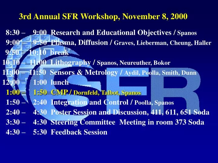
3rd Annual SFR Workshop, November 8, 2000. 8:30 – 9:00 Research and Educational Objectives / Spanos 9:00 – 9:50 Plasma, Diffusion / Graves, Lieberman, Cheung, Haller 9:50 – 10:10 break 10:10 – 11:00 Lithography / Spanos, Neureuther, Bokor

E N D
3rd Annual SFR Workshop, November 8, 2000 8:30 – 9:00 Research and Educational Objectives / Spanos 9:00 – 9:50 Plasma, Diffusion / Graves, Lieberman, Cheung, Haller 9:50 – 10:10 break 10:10 – 11:00 Lithography / Spanos, Neureuther, Bokor 11:00 – 11:50 Sensors & Metrology / Aydil, Poolla, Smith, Dunn 12:00 – 1:00 lunch 1:00 – 1:50 CMP / Dornfeld, Talbot, Spanos 1:50 – 2:40 Integration and Control / Poolla, Spanos 2:40 – 4:30 Poster Session and Discussion, 411, 611, 651 Soda 3:30 – 4:30 Steering Committee Meeting in room 373 Soda 4:30 – 5:30 Feedback Session
Chemical Mechanical Planarization SFR Workshop November 8, 2000 Andrew Chang, Tiger Chang, David Dornfeld, Tanuja Gopal, Edward I. Hwang, Jianfeng Luo, Zhoujie Mao, Costas Spanos, Jan Talbot Berkeley, CA
CMP Milestones • September 30th, 2001 • Build integrated CMP model for basic mechanical and chemical elements. Develop periodic grating metrology (Dornfeld, Talbot, Spanos). • September 30th, 2002 • Integrate initial chemical models into basic CMP model. Validate predicted pattern development. (Dornfeld, Talbot) . • September 30th, 2003 • Develop comprehensive chemical and mechanical model. Perform experimental and metrological validation. (Dornfeld, Talbot, Spanos)
Abstract 2001 Milestone: Build integrated CMP model for basic mechanical and chemical elements. Develop periodic grating metrology Key elements involved in this are: • Chemical Aspects of CMP (J. Talbot and T.Gopal) • Particle Size Distribution in CMP: Modeling and Verification (J. Luo) • Slurry Flow Analysis and Integrated CMP Model (Z. Mao) • Scratch Testing of Silicon Wafers for Surface Characterization (E. Hwang) • Process Monitoring of CMP using Acoustic Emission (A. Chang) • Development of periodic grating metrology (C. Spanos and T. Chang) We will review the recent activities in these areas
Slurry Concentration, Abrasive Shape,Density, Size and Distribution Down Pressure PadRoughness Wafer, Pattern,Pad and Polishing Head Geometry and Material Pad Hardness Relative Velocity SlurryChemicals Chemical Reaction Model (RR0)chem Contact Pressure Model Model of Active Abrasive Number N Model of Material Removal VOL by a Single Abrasive Wafer Hardness Pressure and Velocity Distribution Model (FEA and Dynamics) Fluid Model Physical Mechanism; MRR: N´VOL Preston’s Coefficient Ke (RR0 )mech Dishing & Erosion WIWNU Surface Damage MRR WIDNU Overview of Integrated Model WIWNU
Chemical Aspects of CMPRole of Chemistry - Tanuja Gopal, Jan Talbot UCSD • Chemical and electrochemical reactions between material (metal, glass) and constituents of the slurry (oxidizers, complexing agents, pH) • Dissolution and passivation • Solubility • Adsorption of dissolved species on the abrasive particles • Colloidal effects • Change of mechanical properties by diffusion & reaction of surface
Mass Transfer Processes • (a) movement of solvent into the surface layer under load imposed by abrasive particle • (b) surface dissolution under load • (c) adsorption of dissolution products onto abrasive particle surface • (d) re-adsorption of dissolution products • (e) surface dissolution without a load • Ref. L. M. Cook, J. Non-Crystalline Solids, 120, 152 (1990).
Reaction Chemistries • Dissolution of glass • Dissolution and passivation of W
Generic Chemical Reactions • Dissolution: M(s) + A -> M(aq) + B M(s) + A -> Mn+ + ne- + B • Oxidation: M(s) + O ->M-oxide(s) • Oxide dissolution: M-oxide(s) + A -> M(aq) + B M-oxide(s) + A -> Mn+ + ne- + B • Complexation (to enhance solubility)
Colloidal Effects • Surface charge (zeta potential or isoelectric point, IEP, the pH where the surface charge is neutral) of polished surface and abrasive particle is important (Malik et al.)
Colloidal effects • Maximum polishing rates for glass observed compound IEP ~ solution pH > surface IEP • (Cook, 1990) • Polishing rate dependent upon colloidal particle - W in KIO3 slurries • (Stein et al., J. Electrochem. Soc. 1999)
Experimental Program • Electrochemical/chemical experiments with rotating disk electrode with and without abrasion • Measurement of zeta potential of abrasives as function of pH (IEP) and solution chemistry Potentiostat Coun t e r E l e c t rod e RD E R e fe r enc e E l e c t rod e P o li sh i ng P ad
Modeling of Chemical Effects • Electrochemical/chemical dissolution and passivation of surface constituents • Colloidal effects (adsorption of dissolved surface to particles or re-adsorption) • Solubility changes • Change of mechanical properties (hardness, stress)
Slurry Concentration, Abrasive Shape,Density, Size and Distribution Down Pressure PadRoughness Wafer, Pattern,Pad and Polishing Head Geometry and Material Pad Hardness Relative Velocity SlurryChemicals Chemical Reaction Model (RR0)chem Contact Pressure Model Model of Active Abrasive Number N Model of Material Removal VOL by a Single Abrasive Wafer Hardness Pressure and Velocity Distribution Model (FEA and Dynamics) Fluid Model Physical Mechanism; MRR: N´VOL Preston’s Coefficient Ke (RR0 )mech Dishing & Erosion WIWNU Surface Damage MRR WIDNU WIWNU
Synergistic Effects • MRR = kchem (RRmech)o + kmech (RRchem)o (RRmech)o = mechanical wear = Ke PV (RRchem)o = chem. dissolution = kr exp(-E/RT)PCinKe affected by surface chemical modificationCi affected by mass transport (i.e., V)Ref.:Y. Gokis & R. Kistler,ECS Meeting Abstract 496, Phoenix, Oct. 2000.
Potential Results for Chemical MP Modeling • Selective chemical slurries: 1) control reaction chemistry 2) control colloidal properties of abrasives and removed material3) enhance solubility of removed material • Material wear properties (eg, hardness) • Chemically active pads
Chemical Effects of CMP • Synergistically enhances the rate of material removal with mechanical polishing • Influences the colloidal stability of the abrasive particles • Undesired effects are unwanted etching and dishing of features and increased surface roughness
Effect of Particle Size Distribution in CMP Modeling Abrasive Geometry and Size - J. Luo UCB • Two Abrasive Geometries • Spherical Shape for Obtuse Abrasives • Conical Shape for Sharp Abrasives 100nm X X Schematic of Spherical and Conical Abrasive Shapes in the Model SEM Picture of Slurry Abrasives for Si CMP (Moon, PhD Thesis, 1999) y • Abrasive Size and Size Distribution • Nano-Scale Size X • Normal Distribution (Xavg , )and p((Xavg , ) • Xavg, Xmax and Standard Deviation Xmax Xavg Portion of Active Abrasive Schematic of Abrasive Size Distribution
Role of Abrasive Size in the Architecture of the Integrated CMP Model Contact Mechanics( Pad Topography/Abrasive Size/Pressure ) ? Slurry pH Value and so on Chemical Reaction a12= F2/Hw V = Vol Abrasive Geometry Material Removal Rate Function: MRR= N Vol= C1Hw-3/2 {1-(1-C2P01/3}P01/2V.Correct on both average scale & local single points Schematic of Wafer-Chemical-Abrasive-Pad Interaction to Model the Volume Removed by A Single Abrasive 1 Surface Damage Contact Mechanics( Pad Topography/Abrasive Size/Pressure ) N Abrasive Size Distribution WIWNU Abrasive Geometry Pad Hardness a22= F2/Hp Pressure and velocity distribution over wafer-scale Xmax-Y=2 WIDNU n Pattern Density Schematic of Wafer-Abrasive-Pad Interaction to Model the Number of Active Abrasive Number Detailed Fluid Model
MRR As A Function of Particle Size Distribution Before Saturation (Luo & Dornfeld, 2000) MRR as A Function of Down Pressure and Velocity: MRR= N Vol= C1Hw-3/2 {1-(1-C2P01/3}P01/2V. MRR= C3: A Function of Down Pressure, Velocity, Weight Concentration etc. C4: 0.25(4/3)2/3(1/Hp)Ep2/3/b1P01/3 A Function of Down Pressure, Pad Hardness and Pad Topography. Function p: The probability of the appearance of abrasive size Function : Probability density function. Contribution of Active Particle Number Contribution of Active Particle Size (Larger than Xavg) Contribution of Total Number of Particles over the Wafer-Pad Interface MRR as A Function of Particle Size and Size Distribution
Mean Size (m) Standard Deviation (m) AKP50 0.29 0.070222 AKP30 0.38 0.118959 AKP15 0.60 0.210633 AA07 0.88 0.288768 AA2 2.00 1.056197 Particle Size Distribution Measurement (II) Dynamical Light Scattering *Bielmann et. al. 1999
Particle Size Dependence on MRR: Experiment VS. Model Predictions (0.29, 0.07022) (0.38, 0.118959) (0.60, 0.210633) (0.88, 0.288768) (2.0, 1.056197) C4: 0.25(4/3)2/3(1/Hp)Ep2/3/b1P01/3= 0.015 * Bielmann et. al. 1999
Fraction of Active Particles Based on Model Prediction [0.726, 0.737m] 0.1827% [1.213, 1.231m] 0.1798% [1.720, 1.746m] 0.1815% [0.49, 0.50m] 0.19105% [5.091, 5.169m] 0.1719%
Relationship between Standard Deviation and MRR Based on Model Prediction Number Dominant Region Size Dominant Region
2002 & 2003 Goals Develop comprehensive chemical and mechanical model. Perform experimental and metrological validation, by 9/30/2003. Down Pressure Wafer Smaller contact area Larger contact area H H a
Slurry Flow Analysis and Integrated CMP ModelZhoujie Mao UCBMotivation • Study the effects of slurry flow on the material removal in CMP • Develop integrated process model for CMP to provide insight into the MRR and WIWNU • Develop process model for environmental impact analysis for CMP
Carrier Slurry Slurry feeder Wafer Polishing plate Carrier film Side view Polishing pad Overall Picture of Slurry Flow in CMP • Two flow stages: slurry flow on the polishing pad, slurry flow between wafer and polishing pad
Slurry Flow on the pad Slurry Polishing pad Abrasive particle • Estimate the abrasive particle settling mechanism on the polishing pad • Study the effects of slurry supply rate and slurry delivery position on the material removal rate
Abrasive Particle Settling Rate Vs. Slurry Supply Rate Rate of Deposition (n/m2/s) Radius (mm)
Abrasive Particle Settling Rate Vs. Delivery Position Average Settling Rate Beneath Wafer Eccentricity Average Settling Rate (n/m2/s) Radial Position (mm)
Integrated Slurry Flow Model • Slurry flow between wafer and polishing pad • Slurry flow inside polishing pad • Deformation of wafer • Deformation of polishing pad h(x) hp(x) Pad
2002 & 2003 Goals Develop comprehensive chemical and mechanical model. Perform experimental and metrological validation, by 9/30/2003. • Simulation of Integrated CMP model • Experimental verification of integrated CMP model (role of active abrasives in mechanical material removal)
Scratch Testing of Silicon Wafers for Surface CharacterizationEdward Hwang UCBMotivation • Wafer surface characterization is important to understand and model the material removal mechanism in CMP - Scratch testing supports the identification and verification of surface characteristics of the wafer representative of the CMP process - Scratch testing can give insight on the stress levels occurring during the CMP Process
bulk not affected by the process Si wafer polishing pad layer 1(order of a few nm ) highly hydrated, loosely bound network – lower density Actual CMP Situations Cross Section View layer 2(order of 20 nm ) plastically compressed network – higher density Trogolo et al “Near Surface Modification of Silica Structure Induced by Chemical/Mechanical Polishing”, J. Materials Science 29 (1994) pp. 4554 - 4558
Experimental Setup • Workpiece: Silicon wafer <100> p-type • Pre-CMP Wafers & Post-CMP Wafers • Diamond tool: Nose radius: 48μm • Feed rate: V=399μm/s • Tilt angles: 0.06 degrees. • Acoustic emission sensor: DECI Pico-Z AE sensor • Data collection: 50kHz sampling rate
Layers vs. AE Signals (1) Pre-CMP Wafers AE signals are proportional to the depth of cut in
1.0 0.8 0.6 0.4 0.2 AE Raw Signals (volts) 0.0 -0.2 -0.4 -0.6 -0.8 -1.0 0.00 0.05 0.10 0.15 0.20 0.25 0.30 time(s) Air-cut + Layer 1 Layer 2 Bulk Layers vs. AE Signals (2) Post-CMP Wafers 0.35 Unlike the pre-CMP wafers, post-CMP wafers show discontinuous transitions in the AE signal due to penetration of Layer 2.
Results • Observation of distinct signal changes for transitions between Layer 1 Layer 2 bulk supports surface characterization • Signal for Layer 2 is observed up to 20 nm depth of cut • Highly compressed Layer 2 is more ductile than bulk : - Plastic deformation dominates the material removal mechanism in this regime and should relate to removal rate during CMP • SEM images support the verification of the multi-layered wafer surface
2002 & 2003 Goals Develop comprehensive chemical and mechanical model. Perform experimental and metrological validation, by 9/30/2003. • Replicate the scratch testing with AFM machine in order to be closer to actual CMP situations • Quantify the wafer surface characteristics in CMP
Process Monitoring of CMP using Acoustic EmissionAndrew Chang UCBMotivation • AE monitoring is an applicable diagnostic tool for studying abrasive interaction during CMP • Experimental verification for abrasive particle interaction is needed for CMP modeling • Alternative sensing methods are in-direct (motor current, pad temperature, etc.) or limited to localized areas of the wafer
Acoustic Emission Sources in CMP • Acoustic emission is highly sensitive to abrasive particle interaction between wafer and pad
CMP Tool Toyoda Float Polishing Machine Test Wafers Oxide, aluminum, tungsten, copper blanket wafers Slurry type ILD 1300, abrasive size (~100 nm) W-Slurry, abrasive size (~37 nm) Alumina slurry, abrasive size (~100 nm) Pad type IC 1000/Suba IV stacked pad Polishing Conditions Pressure = ~ 1 psi Table Speed = 20 – 80 RPM Slurry flowrate = 150 ml/min Experimental Setup Pre-amplifier (60 dB) PC Data Acquisition Amplifier (40 dB) RMS Filter RMS AE Raw AE Raw Sampling Rate = 2 MHz RMS Sampling Rate = 5 kHz AE Transducer Wafer
HFpeak Ratio = LFpeak ASL LFpeak Dt AE Ratio Signal Processing ASL HFpeak Dt High Pass Filter >100 kHz Raw AE Signal Low Pass Filter 20-60 kHz
Application to Endpoint Detection • The sensitivity of acoustic emission to various materials during polishing is ideal for endpoint detection in CMP Pad Pad Oxide Wafer Pad
Sensitivity to CMP Process • Background noise characterization • AE is insensitive to low-frequency (audible) noise from CMP tool (motors, belts, etc.) • Sensor location (backside of wafer is ideal) isolates signal from process and filters noise • Signal from process is sensitive to abrasive particle interaction • Signal comparison between deionized water and abrasive slurry • Sensitivity to different materials
2002 & 2003 Goals Develop comprehensive chemical and mechanical model. Perform experimental and metrological validation, by 9/30/2003. • Future tests planned with industrial CMP tool manufacturer • Further experimental tests for validation of integrated CMP model (role of active abrasives in mechanical material removal)
Establishing full-profile metrology for CMP modeling Costas Spanos & Tiger Chang UCB Pattern density mask - MIT 96.4 Feature size 10 m Die size 20mm by 20mm Pattern density ranges from 4% to 100%
Process Flow Get the mask files PECVD oxide ~2mm PSG deposition 1 mm Design contact mask CMP Aluminum 0.7 mm Make emulsion mask Pattern Aluminum The final structure