Download
1 / 29
300 likes | 523 Views
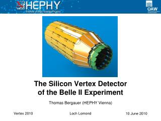
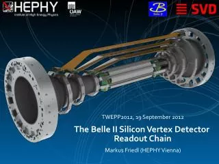
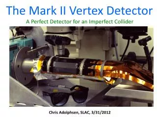
VCI, 13 February 2013. The Belle II Silicon Vertex Detector. Markus Friedl (HEPHY Vienna) for the Belle II SVD Group. Introduction Front-End Electronics Performance Summary. Introduction Front-End Electronics Performance Summary. Belle. KEKB. Linac.

E N D
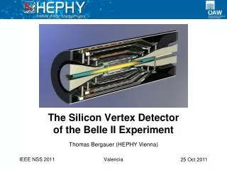
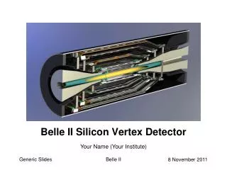
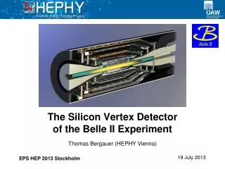
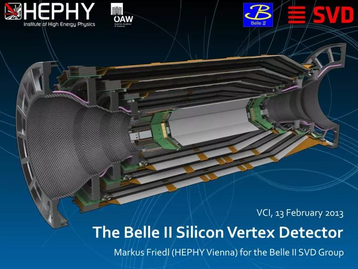
VCI, 13 February 2013 The Belle II Silicon Vertex Detector Markus Friedl (HEPHY Vienna) forthe Belle II SVD Group
Introduction Front-End Electronics Performance Summary M.Friedl (Belle II SVD Group): The Belle II SVD
Introduction Front-End Electronics Performance Summary M.Friedl (Belle II SVD Group): The Belle II SVD
Belle KEKB Linac KEKB and Belle @ KEK (1999-2010) • Center of mass energy: Y(4S) (10.58 GeV) • High intensity beams (1.6 A & 1.3 A) • Integrated luminosity of 1 ab-1 recorded in total • Belle mentioned explicitly in 2008 Physics Nobel Prize announcement to Kobayashi and Masukawa • Asymmetric machine:8 GeVe- on 3.5 GeVe+ Belle KEKB ~1 km in diameter Linac About 60km northeast of Tokyo M.Friedl (Belle II SVD Group): The Belle II SVD
SuperKEKB/Belle II Upgrade: 2010–2015 • Aim: super-high luminosity ~81035 cm-2s-1 11010 BB / year • LoI published in 2004; TDR published in 2010 • Refurbishment of accelerator and detector required • nano-beams with cross-sections of ~10 µm x 60 nm • 10 mm radius beam pipe at interaction region http://belle2.kek.jp M.Friedl (Belle II SVD Group): The Belle II SVD
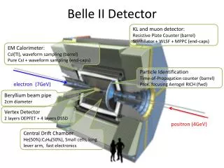
Belle II VertexingSubdetectors Pixel Detector (PXD) 2 layers of DEPFET pixels Silicon Vertex Detector (SVD) 4 layers of DSSDs M.Friedl (Belle II SVD Group): The Belle II SVD
Belle II Vertexing Environment • Low energy machine (10.58 GeV) – multiple scattering • Needs very low mass detector • PXD DEPFET sensors are thinned to 75 µm • SVD uses “Origami chip-on-sensor” concept • High luminosity – occupancy/pile-up • Need small sensitive area and/or fast readout • PXD has small cell size (50 x 50 µm2) • SVD has fast shaping (50 ns) and hit time reconstruction (~3 ns) • Radiation – 100 kGy • Magnetic field – 1.8 T M.Friedl (Belle II SVD Group): The Belle II SVD
Silicon Vertex Detector Concept • Use largest possible (6”) double-sided sensors (DSSDs) • Minimize relative amount of structural material • Fast shaping readout • Minimize occupancy • Fast readout implies higher noise • Noise is mainly determined by input capacitance • Place readout chips as close as possible to sensor strips • Minimize capacitive load by avoiding long fanouts • Use efficient CO2 cooling • Allows thin cooling pipes M.Friedl (Belle II SVD Group): The Belle II SVD
Belle II Vertex Detector • Pixel Detector – 8M pixels • 2 DEPFET layers at r = 14, 22 mm • Excellent and unambiguous spatial resolution (~15 µm) • Coarse time resolution (20 µs) • Silicon Vertex Detector – 220k strips • 4 DSSD layers at r = 38, 80, 104, 135 mm • Good spatial resolution (~12/25 µm) but ambiguities due to ghosting • Excellent time resolution (~3 ns) • Combining both parts yields a very powerful device! M.Friedl (Belle II SVD Group): The Belle II SVD
Introduction Front-End Electronics Performance Summary M.Friedl (Belle II SVD Group): The Belle II SVD
Front-End Geometry • 4 layers arranged in ladders • Outer 3 layers have slanted forward part • Limited acceptance angle (17°…150°) allows to place services outside (cyan cones) while minimizing material within M.Friedl (Belle II SVD Group): The Belle II SVD
Double-Sided Silicon Sensors • 3 different types required • Large rectangular sensors – 123 x 58 mm2 (HPK) • Small rectangular sensors – 123 x 38 mm2 (HPK) • Trapezoidal sensors – 123 x 58…38 mm2 (Micron) • Production is in progress • Presently ~60% delivered M.Friedl (Belle II SVD Group): The Belle II SVD
Origami Chip-on-Sensor Concept • Low-mass double-sided readout • Flex fanout pieces wrapped to opposite side • All chips aligned on one side single cooling pipe (D = 1.6 mm) Side View (below) M.Friedl (Belle II SVD Group): The Belle II SVD
Origami Prototype Modules • Single Origami module • Double Origami module M.Friedl (Belle II SVD Group): The Belle II SVD
Sensor underneath flex circuit End ring (support) APV25 chips Origami ladder Pitch adapter bentaround sensor edge Cooling pipe M.Friedl (Belle II SVD Group): The Belle II SVD
Introduction Front-End Electronics Performance Summary M.Friedl (Belle II SVD Group): The Belle II SVD
General SVD Readout Scheme • Based on existing prototype system (2007) verified in lab and beam tests DATCON ONSEN Finesse Transmitter Board (FTB) FADC 1748APV25chips ~2mcoppercable Junctionbox ~10mcopper cable Unified opticaldata link (>20m) COPPER Front-endhybrids Rad-hardDC/DC converters Analog level translation,datasparsificationandhit time reconstruction Unified Belle IIDAQ system M.Friedl (Belle II SVD Group): The Belle II SVD
APV25 Front-End Chip • Developedfor CMS by IC London and RAL • 70,000 chipsrunning in the CMS Trackersince 2008 • 40 MHz clock; 128 channels; 192 cellsdeep analog pipeline • 50 ns (adjustable) shaping time • 0.25 µm CMOS process (>100 MRad tolerant) • Low noise: 250 e + 36 e/pF • Multi-peakmode (read out severalsamplesalongshapingcurve) M.Friedl (Belle II SVD Group): The Belle II SVD
Junction Box • CERN-made DC/DC converters for front-end powering • Comparative measurement: no noise penalty M.Friedl (Belle II SVD Group): The Belle II SVD
FADC Block Diagram • Analog & digital level translation between bias and GND • Digitization, signal conditioning (FIR filter), data processing • Central FPGA is an AlteraStratix IV GX M.Friedl (Belle II SVD Group): The Belle II SVD
FADC: Overall Concept • 9U VME module (needs much space for level translation circuits) • Circuit is designed, now PCB layout is made M.Friedl (Belle II SVD Group): The Belle II SVD
The “Human” Touch… M.Friedl (Belle II SVD Group): The Belle II SVD
FTB: Link to DAQ and PXD • Firmware development ongoing • Optical link tests at 2.54 and 3.175 Gb/s successful • Second iteration of PCB for minor corrections underway • SVD data are also streamed to PXD for online data reduction M.Friedl (Belle II SVD Group): The Belle II SVD
Introduction Front-End Electronics Performance Summary M.Friedl (Belle II SVD Group): The Belle II SVD
Hit Time Reconstruction Benefits Belle I SVD • Sufficient to cope with a 40-fold increase in luminosity Belle II SVD M.Friedl (Belle II SVD Group): The Belle II SVD
Achieved Hit Time Resolution • Results achieved in beam tests with several different types of Belle IIprototype modules (covering a broad range of SNR) • 2...3 ns RMSaccuracy at typical cluster SNR(14...24) • Will be donein FPGA (using lookup tables) – simulationsuccessful Close to theoretical limit (G. De Geronimo, in “Medical Imaging” by K. Iniewski) M.Friedl (Belle II SVD Group): The Belle II SVD
Z Vertex Resolution • Belle II (PXD & SVD) will be a factor 2 better than Belle (SVD only) M.Friedl (Belle II SVD Group): The Belle II SVD
Introduction Front-End Electronics Performance Summary M.Friedl (Belle II SVD Group): The Belle II SVD
Summary • Belle II Vertex Detector consists of • Pixel Detector (PXD): unambiguous spatial resolution • Silicon Vertex Detector (SVD): precise timing • Silicon Vertex Detector • 4 layers of 6” double-sided silicon sensors • APV25 front-end chip with 50 ns shaping time • Origami chip-on-sensor readout concept for low mass • Highly efficient CO2 cooling • Schedule • R&D completed, construction has started • Now building final prototypes (pre-series) M.Friedl (Belle II SVD Group): The Belle II SVD