Download
1 / 9
130 likes | 566 Views
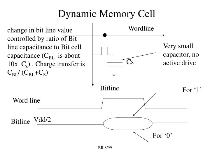
Dynamic Memory Cell. Wordline. change in bit line value controlled by ratio of Bit line capacitance to Bit cell capacitance (C BL is about 10x C s ) . Charge transfer is C BL / (C BL +C S ). Very small capacitor, no active drive. Cs. Bitline. For ‘1’. Word line. Vdd/2. Bitline.

E N D
Dynamic Memory Cell Wordline change in bit line value controlled by ratio of Bit line capacitance to Bit cell capacitance (CBL is about 10x Cs) . Charge transfer is CBL/ (CBL+CS) Very small capacitor, no active drive Cs Bitline For ‘1’ Word line Vdd/2 Bitline For ‘0’ BR 8/99
DRAM Comments • Voltage swing on Bitline is small • Want Bitline capacitance as small as possible, Bit cell capacitance as large as possible to increase charge transfer • Read is destructive – part of read cycle is used to restore level inside of bit cell capacitor • Capacitor leaks, must be refreshed periodically • Noise sources in DRAM are word line to bit line coupling, bit line to bit line coupling BR 8/99
DRAM Layout† Cell 2 x 4 features! Actual size for 256 Mb DRAM cell in 0.22 um reported as 0.484um x 0.968 um ( 2.2F x 4.4F) †Okuda, “A Four-level Storage 4GB DRAM”, IJSCCS Vol 32, No11, Nov 1997 BR 8/99
Open Bitline Architecture EQ WL1 WL0 WLD’ WLD WL0’ WL1’ CWBL + SA - BL BL’ C C C C C C CBL CBL’ dummy cells EQ raised, and LD, LD’ also raised to precharge bitlines and dummy bit cells to Vdd/2 . During read, if cell from left hand side is read (raise WL1), then dummy word line on right cell is raised. Raising a word line couples noise into bitline, want same noise injected on both lines (only the same if both signals are matched, and bitlines are matched). BR 8/99
Folded Bitline Architecture -- more noise suppression WLA WLB WLC WLD WLD’ Cell BL Pair to SA BL’ BL Pair to SA BL’ No Cell 4F 2F Cell is connected to BL or BL’ on every other column. WLD, WLD’ are dummy bit lines. Assume WLA is driven. Then WLD is driven; if WLB is driven, then WLD’ is driven. BR 8/99
Folded Bit lines – more noise suppression • normal word lines (WLA, WLB, etc) and dummy word lines (WLD, WLD’) cross both bitlines • Even if signal characteristics of both word lines differ substantially, same coupling noise from both is coupled into both bitlines, which appears as common mode to SA, which rejects it. • bitlines more closely matched since they run side-by-side • However, bitlines in folded architecture are somewhat longer than non-folded bitlines, so bit line capacitance is higher, reducing charge transfer from cell. BR 8/99
Bit Line to Bit Line Coupling - SA + BL2 Ccross BL1’ - SA + BL1 Ccross BL0’ - SA + Signal coupling from BL2, BL0’ will effect bit line voltages on BL1’, BL1 BR 8/99
Transposed Bit lines - SA + BL2 Ccross Ccross Ccross Ccross BL1’ - SA + BL1 Ccross Ccross Ccross Ccross BL0 - SA + Does not reduce noise coupling, but couples same noise into both bitlines so appears as common node noise and is rejected. BR 8/99
Capacitor Design • To achieve density for Mb, Gb DRAMs, capacitors had to go 3D • CUB – Capacitor under Bitline • Trench capacitor, sidewall of trench used to form capacitor plate • Used up to 16Mb DRAM • COB – Capacitor Over Bitline – stacked capacitor • Used in 64Mb+ DRAMs • Forms a 3D cylindrical capacitor in which both inside and outside surfaces can be used • Memory cell array at a different (higher) height than surrounding surfaces, can cause metallization problems. BR 8/99