Download

1 / 14
140 likes | 270 Views
Electrical Evaluation of Electron Traps in Hf-based Gate Stacks. G. Bersuker C. Young D. Heh R. Choi. Pulse Id-Vg Technique. Example. Ultra-Short pulse measurement allows determination of the “onset of trapping”

E N D
Electrical Evaluation of Electron Traps in Hf-based Gate Stacks G. Bersuker C. Young D. Heh R. Choi
Pulse Id-Vg Technique Example • Ultra-Short pulse measurement allows determination of the “onset of trapping” • Detectable trapping was not observed until tp 100 ms for the gate stacks in this study • The DVt is calculated as in: Bersuker et al, 2004 Spring MRS, APL 2005 02/16/05
Pulse v DC Id-Vg 700 ] Chem Ox/3 nm IN HfO /TiN 2 A*nm 600 m V = 100mV [ 500 d 400 EOT = 1.15 nm 300 Drain Current * EOT o N , 600 C 2 200 100 DC Pulse 0 0.0 0.4 0.8 1.2 1.6 2.0 Gate Voltage [V] • Ramped pulse Id-Vg done with tr = tf = 2 ns and PW = 35 ns 02/16/05
Pulse Mobility • Pulse mobility extraction using Pulse Id-Vg in conjunction with NCSU CVC and Mob2d 02/16/05
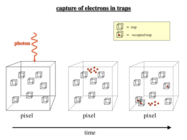
C A A B 0 V 0 Si Si Si Si Si Si 0 V V 0 V k k k k Gate Gate Gate Gate Gate Gate SiO SiO SiO SiO SiO SiO High High High High High High - - - - - - k k 2 2 2 2 2 2 Electrode High-k SiO2 Charge Trapping Model • Fast process: direct resonance tunneling of injected electrons into the traps • Slow process: migration of trapped electron to unoccupied traps 02/16/05
Fast Electron Trapping Process 20 t = t = 100 ns PW = 100 m s r 350 f 77K 150K T= 298-150K 15 300 Current [mA] ] A 225K 10 m [ 250 d I D 298K 5 200 tr/f =100ns, PW=100ms V = 1.8 V g 0 150 0 5 10 15 0 50 100 150 200 250 ] [ m s Time [ms] Pulse Time Flux n=N0(1-e-pt) Trap capture cross-section & density: σ E-14 cm2, N0 E14/cm2 02/16/05
Slow Electron Trapping Process V =1.80V g 298K 0.02 225K Delta Vt (V) 0.01 150K 77K 0 0 200 400 600 800 1000 1200 Time (sec) V V =1.95V =1.95V g g 298K 298K 0.02 Delta Vt (V) 225K 225K 0.01 150K 150K 77K 77K 0 0 200 400 600 800 1000 1200 Time (sec) Fast trapping component is subtracted N0=109–1010 cm-2 02/16/05
O Hf V 0 Nature of Bulk Traps: O vacancies Negative oxygen vacancies Energy: V- 0.5 eV; V-2 0.3 eV; Dimension: 1 nm 02/16/05
Resonance Injection Points in Pulse Measurement • HfO2-SiO2 offset of 2.3 eV is used for band alignment (IFIGS model, R. Nemanich, GSEWG meeting, 02/06) 02/16/05
Electron Trap Profile in High-k Layers • Electron traps uniformly distributed across the high-k film thickness • No significant difference in trap density between deposition methods and anneal ambients 02/16/05
Frequency Dependent Charge Pumping measurements DC I-V Charge Pumping • CP: Discharge is done immediately after CVS to de-trap any trapped electrons • DC I-V: Represents DC Id-Vg that are taken intermittently between 0 and 300 seconds • 10 second discharge at the end of stress cycle 02/16/05
Charge Pumping Energy and Spatial Probing F x(Å) Et-Ei (eV) 2 kHz x(Å) 1 MHz Et-Ei (eV) Spatial/energy range probing by CP at a given frequency 02/16/05
Electron Trap Depth profile • Factors affecting conversion of frequency to distance: • Capture cross sections decrease exponentially with depth • Recombination rate is limited by the capture of holes 02/16/05
Recovery of the Generated Traps • Generated defects can be passivated using FGA at 450°C for 30 min • Subsequent stress re-activates passivated defects 02/16/05