Download
1 / 33
620 likes | 2.3k Views
Sputtering Processes for Thin Film Deposition. Suiqiong Li ELEC 7730 Instructor Dr. Y. Tzeng. Outline. Fundamentals of sputtering Techniques of sputtering DC sputtering RF sputtering Magnetron Sputter Deposition Reactive sputtering Sputtering zinc oxide thin film. Questions.

E N D
Sputtering Processes for Thin Film Deposition Suiqiong Li ELEC 7730 Instructor Dr. Y. Tzeng
Outline • Fundamentals of sputtering • Techniques of sputtering • DC sputtering • RF sputtering • Magnetron Sputter Deposition • Reactive sputtering • Sputtering zinc oxide thin film
Questions • Compare with DC sputtering, what are the advantages of RF sputtering? • What parameters would affect sputter yield?
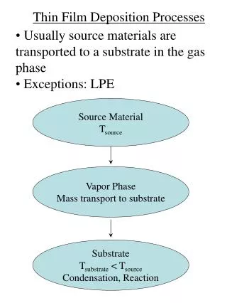
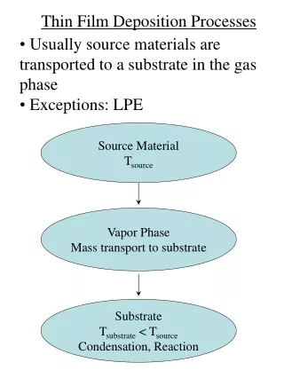
The Mechanisms of Sputtering • Interactions of ions with surfaces The ion impact may set up a series of collisions between atoms of the target, possibly leading to the ejection of some of these atoms. This ejection process is known as sputtering. http://www.postech.ac.kr/mse/tfxs/2003_2/chapter3.pdf
Sputtering Deposition Process • Sputtering • Ions are accelerated into target • Some of the surface atoms are sputtered off of the target. • These sputtered atoms “flow” across the chamber to where they are deposited http://www.utdallas.edu/~goeckner/plasma_sci_class/Plasma%20Process%203%20Types.pdf
Sputter Yield Sputtering process is characterized by sputter yield (S) S values are typically in the range of 0.01 and 4 and increase with the mass of metals and energy of the sputtering gas. http://matlb.kjist.ac.kr/~master/lecture/TFT/PVD2(14).ppt
Sputter Yield (Cont.) The sputter yield depends on: (a) the energy of the incident ions; (b) the masses of the ions and target atoms; (c) the binding energy of atoms in the solid and (d) the incident angle of ions. 60o – 70o http://www.postech.ac.kr/mse/tfxs/2003_2/chapter3.pdf
Sputtering Alloy Targets composition of alloy in film is approximately the same as alloy in target (unlike evaporation) • slow diffusion mixing in solids (sputtering) • target reaches steady state • surface composition balances sputter yield http://www.postech.ac.kr/mse/tfxs/2003_2/chapter3.pdf
Advantages of sputter deposition • Elements, alloys and compounds can be sputtered and deposited. • The sputtering target provides a stable, long-lived vaporization source. • In some configurations, reactive deposition can be easily accomplished using reactive gaseous species that are activated in plasma. • The source and substrate can be spaced close together. • The sputter deposition chamber can have a small volume. http://www.pfonline.com/articles/069901.html
Disadvantages of Sputter Deposition • Sputtering rates are low compared to those that can be attained in thermal evaporation. • Sputtering targets are often expensive and material use may be poor. • Most of the energy incident on the target becomes heat, which must be removed. • In reactive sputter deposition, the gas composition must be carefully controlled to prevent poisoning the sputtering target. http://www.pfonline.com/articles/069901.html
Sputtering System The Vacuum Sputtering System http://www.ece.rochester.edu/research/cleanroom/Main/Facilities/sputterpic.htm
Basic Techniques • DC (diode) sputtering • RF (radio frequency) sputtering • Magnetron sputtering • Reactive sputtering
DC Sputtering The simplest sputtering technology • E (e-) < 2eV - no ionization, elastic collisions only • E (e-) > 2eV - inelastic collisions add energy to Ar • ionization (highest energy process, ~15eV) • Note: mass (e-)/mass( Ar) ~ 10-5 • energy transfer small • e- gain energy via elastic collisions until E>15eV for ionization • #ions ~ #neutrals ~ 3 x 109 cm-3 @ 10mT http://www.glue.umd.edu/~ddev/me489f/slides/2b_deposition_x6.pdf
DC Sputtering (Cont.) Light e- pulled towards walls faster than ions, leaving slightly more ions in glow region Light e- move away from cathode faster than ions, leading to a large field, high acceleration of ions into cathode high-E ions (10keV to 1 MeV) knock target material loose resulting plume of neutrals new electrons from impact reactions replenish the plasma http://www.glue.umd.edu/~ddev/me489f/slides/2b_deposition_x6.pdf
Operating Pressure for DC sputtering Operating pressure limitations are imposed by the requirement of both the glow discharge and of film deposition. Optimum deposition rate around 100 mTorr Milton Ohring, Materis Science of Thin Film, second Edition, P208
Parameters for DC Sputtering • Sputter voltage • typically -2 to -5 kV • Substrate Bias Voltage • substrate is being bombarded by electrons and ions from target and plasma • sputtering film while you deposit • neutral atoms deposit independently • put negative bias on the substrate to control this • can significantly change film properties • Deposition rate • changes with Ar pressure • increases with sputter yield • usually increases with high voltage http://www.uccs.edu/~tchriste/courses/PHYS549/549lectures/sputtertech.html
RF Sputtering • DC sputtering - what about dielectrics? • in DC systems, positive charge builds up on the cathode (target) need 1012 volts to sputter insulators !! avoid charge build up by alternating potential RF sputtering http://www.uccs.edu/~tchriste/courses/PHYS549/549lectures/sputtertech.html
Target Self-Bias Dueto the different masses, electrons can be accelerated to oscillate with the RF, while ions are to heavy and react only on the averages generated in the RF system. It behaves like a DC target where positive ion-bombardment sputters away atoms for subsequent. Milton Ohring, Materis Science of Thin Film, second Edition, P214
RF Sputtering • frequencies less than about 50 kHz • electrons and ions in plasma are mobile • both follow the switching of the anode and cathode • basically DC sputtering of both surfaces • frequencies above about 50 kHz • ions (heavy) can no longer follow the switching • enough electrons to ionize gases(5~30MHz) Typically 13.56 MHz is used
Electrode-Size Effects • Both electrodes in RF sputtering system should sputter. cause a contamination in the sputtered film. • The ratio of the voltage across the sheath at the small capacitively coupled electrode(Vc) to that across the large directly coupled electrode(Vd) including substrate and chamber walls, etc is given by The fourth- power dependence means large Ad is very effective in raising the target sheath potential while minimizing ion bombardment of grounded fixtures. substrate and chamber make a very large electrode - so not much sputtering of substrate
Advantages of RF Sputtering • It works well with insulating targets • High efficiency easier to keep plasma going → can operate at lower Ar pressures (1-15 mTorr) → fewer gas collisions → more line of sight deposition http://aultimut.com/aultimut/details.asp?itemid=11
Magnetron Sputter Deposition • Use with DC or RF • High sputtering efficiency increase ionization of Ar • Why? Higher sputter rates at lower Ar pressures (down to 0.5 mTorr) fewer gas collisions - more line of sight • How ? increase probability of electrons striking Ar • increase electron path length • use electric and magnetic fields
Magnetron Sputtering Principle This technology uses powerful magnets to confine the “glow discharge” plasma to the region closest to the target plate. That vastly improves the deposition rate by maintaining a higher density of ions, which makes the electron/gas molecule collision process much more efficient. http://www.angstromsciences.com/technology/sputtering.htm
Advantages of Magnetron Sputtering • High deposition rate • Reducing electron bombardment of substrate • Extending the operating vacuum range • ability to operate at lower pressures The most widely commercially practiced sputtering method
Parameters for Magnetron Sputtering • Deposition pressure : 10-3 to 0.1 Pa ( 10-5 to 10-3 torr) • Deposition rate : 0.2 ~ 2-6 m/min (10 times higher than conventional sputtering) • Deposition temperature : 100 to 150 oC http://engineering.dartmouth.edu/other/microeng/courses/es194/student/jiaying/sem/II.2.p4.html
Disadvantages for Magnetron Sputtering • An erosion track in the target • his leads to poor efficiency of sputtering yield versus target volume compared to non-magnetron sputtering • Nonuniform removal of particles from target result in nonuniform films on substrate http://www.mse.ncsu.edu/WideBandgaps/classes/MAT%20751%20S03/Sputtering/Magnetron_Ihlefeld.pdf
Reactive Sputtering Sputtering metallic target in the presence of a reactive gas mixed with inert gas (Ar) • A mixture of inert +reactive gases used for sputtering oxides – Al2O3, SiO2, Ta2O5 (O2) nitrides – TaN, TiN, Si3N4 (N2, NH3) carbides – TiC, WC, SiC (CH4, C2H4, C3H8)
Reactive Sputtering (Cont.) • chemical reaction takes place on substrate and target • can poison target if chemical reactions are faster than sputter rate • adjust reactive gas flow to get good stoichiometry without incorporating excess gas into film
Reactive Magnetron SputteringZinc Oxide Thin films • Zinc oxide is one of the most interesting II/IV compound semiconductors It has been investigated extensively because of its interesting electrical, optical and piezoelectric properties Reactive sputtering is the best technique for Zinc Oxide deposition. R. Ondo-Ndong , F. Pascal-Delannoy, A. Boyer, A. Giani, A. Foucaran, Materials Science and Engineering B97 (2003) 68 /73
Process Parameters • The physical properties of ZnO films are influenced not only by the deposition techniques, but also by process parameters. The film deposited on high temperature substrate will show finer uniform grains and smoother surface Walter Water, Sheng-Yuan Chu*, Materials Letters 55 (2002) 67– 72
Process Parameters Quality of the film dependents on deposition conditions, such as substrate temperature, deposition power, deposition pressure and argon–oxygen flow. Walter Water, Sheng-Yuan Chu*, Materials Letters 55 (2002) 67– 72
Conclusion • Sputter deposition, also known as physical vapor deposition, or PVD, is a widely used technique for depositing thin metal layers on semiconductor wafers. • The range of applications of sputtering and the variations of the basic process, is extremely wide.
Questions Answer • It works well with insulating targets; High efficiency • The sputter yield depends on: (a) the energy of the incident ions; (b) the masses of the ions and target atoms; (c) the binding energy of atoms in the solid and (d) the incident angle of ions.