Download
1 / 49
630 likes | 1.38k Views
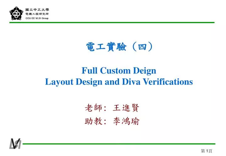
電工實驗 ( 四 ) Full Custom Deign Layout Design and Diva Verifications. 老師 : 王進賢 助教 : 李鴻瑜. Outline. Cross Section & Layout View Layout (Design) Rules Layout Edit Diva Verifications (DRC/LVS). gnd. Vin (Poly). Vout. Polysilicon. vdd. thin Oxide. p+. n+. n+. p+. p+. n+. Butting

E N D
電工實驗 (四) Full Custom DeignLayout Design and Diva Verifications 老師: 王進賢 助教: 李鴻瑜
Outline • Cross Section & Layout View • Layout (Design) Rules • Layout Edit • Diva Verifications (DRC/LVS)
gnd Vin(Poly) Vout Polysilicon vdd thin Oxide p+ n+ n+ p+ p+ n+ Butting contact Butting contact P WELL N WELL P substrate gnd vdd Vin (Polysilicon) N WELL contact Pimp Nimp Vout Nimp Pimp CMOS 的反相器的橫截面圖與佈局(layout)圖 Cross Section V.S. Layout View
Extension Extension Space Width Space Overlap Enclosure Definition For Parameters Of Layout Rules 基本定義 (Definition) 1.請記住這些名稱的定義 2.接下來所介紹的 layout rules 必須熟記在心, 在劃 layout 時務必遵守這些規則。
1.c 1.a 1.b 1.a n+ NW NW 1.c Metal 1 n+ PW:沒有被NW包圍 的區域都視為 P well NW Layout (Design) Rules (I) 1. NW (N well) 這個 NW的電位 與左邊二個 NW 的電位是不同的, 因為沒有任何的 導線做為連接。 這二個 NW 是同電位的, 因為由 Metal 1 做為導線連接 單位為um
2.e/2.f 2.a 2.b 2.b n+ 2.c 2.g 2.c p+ p+ 2.h Poly Poly 2.a 2.c 2.i p+ p+ n+ 2.c n+ 2.j 2.d n+ p+ 2.j 2.j n+ NW 2.j p+ PW Layout (Design) Rules (II) 2. OD (thin oxide) 單位為um
3.g 3.f 3.a or 3.b PO PO 3.d PO 3.d 3.e 3.g n+ / p+ n+ / p+ 3.e 3.c Layout (Design) Rules (III) 3. PO (Poly) 單位為um
4.h PP 4.a PP OD OD p+ p+ 4.c n+ 4.b OD 4.d PP 4.f p+ p+ PO p+ 4.e p+ 4.g 4.i n+ NP 4.i Layout (Design) Rules (IV) 4. PP (P implantation) NP(N implantation) 單位為um
OD 5.e 5.g n+ p+ 5.c 5.e 5.g PO 5.b 5.i p+ 5.a 5.k n+ PO OD 5.d n+ n+ 5.f 5.j Layout (Design) Rules (V) 5. CO (contact) 單位為um
current >10um 6.a M1 6.d 6.d 6.d 6.d M1 M1 6.a 6.c 6.b M1 CO M1 Layout (Design) Rules (VI) 6. M1 (Metal 1) 單位為um
7.i 7.g 7.d >10um VIA VIA CO 7.f 7.e M1 PO VIA 7.h OD 7.a VIA 7.b VIA 7.c M1 Layout (Design) Rules (VII) 7. VIA (VIA 1) 單位為um
8.e current >10um VIA 8.a M2 8.d 8.d 8.d 8.d M2 M2 8.a 8.c 8.b M2 VIA M2 Layout (Design) Rules (VIII) 8. M2 (Metal 2) 單位為um
9.d VIA2 VIA2 9.e 9.a 9.a 9.a >10um VIA1 9.b 9.b VIA2 M2 VIA2 VIA2 M3 9.c M1 M2 M3 Layout (Design) Rules (IX) 9. VIA 2 單位為um
10.d current >10um VIA2 10.a M3 10.e 10.e 10.e 10.e M3 M3 10.a 10.c 10.b 10.b M3 VIA2 M3 Layout (Design) Rules (X) 10. M3 (Metal 3) 單位為um
Outline • Cross Section & Layout View • Layout (Design) Rules • Layout Edit • Diva Verifications (DRC/LVS)
Create New Library (I) 游標指到此處空格內,填入 Library Name後按 OK
Create New Library (II) 按 OK 如果沒有, 可以重新Refresh 再確認一次 填入technology file, 按OK後執行Compiler 檢查是否Create成功
Create Schematic View and Circuit 設計並完成Schematic 填入Cell name 和schematic
Create Layout View 選擇欲編輯的library 應會自動選擇為 Virtuoso(即Layout Editor) 鍵入Cell name 和layout 將滑鼠游標移至各icon上, 可以看到各種快捷功能說明
滑鼠的座標 與上一點的相對位置 目前使用中的command 放大縮小的快速圖示 (Zoom In and Zoom out) 修改、複製及移動的快速圖示 (Strech, copy and move) 這些是編輯時的快速圖 示,也可以使用 hot key, 在編輯時可以配合 Shift 做 加選及 Ctrl 做少選。 量尺寸的快速圖示或按k 鍵,而清除尺寸按K鍵。 Edit Layout 編輯layout時,建議盡量使用hot key (即Bind key),以增加 layout速度
LSW (Layer Select Window) 目前所選用的層 Library name 設定instance, pin 是否可編輯 All Select and No Select All View and No View 各種Layer可複選成 可視或可選擇 LSW主要用在Layout時, 配合各種layer的選取, 以方便編輯
Layers and display.drf 根據 Technology file 內所定義的 Layer name 與 Layout rule 中的 Layer name 之名稱對映。 display.drf file NW (N Well) OD (thin oxide) PP (P implantation) NP(N implantation) PO (poly) M1 (metal 1) VIA (VIA 1) CO (contact) M2 (metal 2) 注意,在 Technology file內所定義的每一個 Layer name 皆會對映一個 Layer number 。有的 Layer name 會有 dg(drawing) 與 pn(pin) 兩種不同的屬性定義,主要的差別 是 purpose的定義不同,如dg 是252,而pn 是251。 一般 畫 Layout 是使用 dg 的,只有在宣告為pin 腳時才使用 pn。
Set Display Options 開啟Display Options 來設定Grid。一般 Grid 的設法為所有 layout rules 裡的最小 單位,在此設為 0.05 若是 Grid 沒有設好, 則在畫 layout 時將會 有很多的困擾,更嚴 重可能會有 error 的情 形,所以每次開始畫 layout 時請務必先做好 設定。 是否顯示Pin的 Access Edge 設定編輯時游標 可以移動的方向
Open and Edit Layout 使用滑鼠中鍵按住 點選或雙擊layout, 可以開出編輯視窗
Set Editor Options 取消點選避免游標被 吸引到layer 的邊線 將環境設定到環境檔
Start Layout 從一個 schematic 開 始,設計到 layout, 最好事先做好佈局 的規劃,如右邊條 形圖( symbolic diagram ),先簡單 粗略的擺設,使其 能善用空間,做到 使用最少的 pitch 數. 一個 pitch 最多 只能存在一個 輸出或輸入的 pin。此為“and5” ,共有 6 個輸出 入 pin,而 layout 的結果也只使 用 6 個 pitch 數 ,所以最省空間.
先至 LSW 內選好要畫的層,在此假設 METAL 1 • 接著按 r 鍵並配合 mouse 的左鍵 click 做為 • 起點,而托曳 mouse 即可劃出一個如左圖的矩形。 • 再到 LSW 內選擇 GPOLY 後同上方式,用 mouse • 就可以再畫出一個左圖矩形的 polysilicon。 • 按 u 鍵可以取消前一個動作,而按 ESC 鍵則取 • 消目前的這個命令;每次更換命令最好按 ESC。 • stretch:先用 mouse 輕點 METAL 1 矩形的某一邊, • 之後按 s 鍵並配合 mouse 即可改變矩形的大小。 • move:任意選擇所要搬移的目標,之後按 m 鍵 • 並配合 mouse 即可。 • chop:任意選擇所要分割 • 的矩形,之後按 shift + c 鍵 • ,再利用 mouse 來剪開矩形 • merge:只限於相同的層 • 任意框選所要結合 • 的矩形,或利用shift • 來加選,等確定後 • 按 shift + m 即可 • 按 k 鍵配合 mouse 可以畫出尺規線 • ,而按 shift + k 鍵則清除尺規線。 目前命令的說明 Practice Layout (I)
畫 layout 必須有層次的先後關念,例如一個訊號從 poly 輸入,而從 metal 2 輸出, 就必須先畫 poly 再疊上 contact,再疊上 metal 1,再疊上 via,最後再疊上 metal 2。 其過程缺一不可。如下所示: (contact) (poly) (metal 1) (poly 到 metal 1) (via) (poly 到 metal 1) (metal 2) (poly 到 metal 2) (poly 到 metal 2) (pin) (poly 到 metal 2 加輸出 pin) poly 輸入 metal 2 的 pin 輸出 Practice Layout (II)
Practice Layout (III) 另一種方法比較節省面積,就是 via 與 contact 重疊在一起。同樣的例子, 如一個訊號從 poly 輸入,而從 metal 2 輸出。如下所示: (contact) (poly) (metal 1) (poly 到 metal 1) (via) (poly 到 metal 1) (metal 2) • (poly 到 metal 2) • contact 被 via 完全包住 (poly 到 metal 2) (pin) (poly 到 metal 2 加輸出 pin) poly 輸入 metal 2 的 pin 輸出
現 在 來 學 習 加 pin 吧 , 開 始 若要再察看 pin 的屬性,只要用先選好 pin 後按 q 鍵即開出如下的視窗,選擇 connectivity 便可察看甚至修改。 注意: metal 2 (pn)層 ,而非 (dg)層 Create Pin
Feedthrough pin 的建立 此為 Feedthrough pin 其基本組合 如下: 此為設定 pin 時的 參考,建立過程請 參考上一頁,值得 注意的是 I/O Type 選 jumper 而 Name 任意取名,但不重複 Create Feedthrough
Finished Layout • 一般注意事項: • 輸出入 pin 盡量拉至 cell 中心 • 兩個 pin 的中心點相互間的距 • 離是一個 pitch • 最外面的二個 pin中心點與 • boundary 的距離是二分之一個 • pitch • 盡量加 Feedthrough pin • 盡量加 WELL contact • pmos 及 nmos 的 drain 端在 • layout 時盡可能靠近,使其 • 面積為最小
Outline • Cross Section & Layout View • Layout (Design) Rules • Layout Edit • Diva Verifications (DRC/LVS)
Verifications • Circuit layout 完成後所須作的驗証如下: • DRC (Design Rule Check): • 對 IC 的佈局(layout) 作幾何空間的檢查以確保線路能 • 夠被特定的製程技術所實現。 • ERC (Electrical Rule Check): • 檢查 power, ground 的 short, floating device, floating net • 等指定的電氣特性。 • LVS (Layout Versus Schematic): • 將 layout 與 schematic 作比對,以檢查電路的連接,與 • MOS 的 Length、Width 值是否配。 • LPE (Layout Parameter Extarction): • 從 layout database extract 電氣參數 (如 MOS 的 W、L 值 • ,BJT,diode 的 area,perimeter,node 的 parastic cap.) • ,並以 HSPICE netlist 方式表示電路。
Diva Versus Dracula • 光罩或製程在 IC 製過程中是相當昂貴的,所以佈局驗証的重要性 • 自然是不可言喻,一般佈局驗証包括 DRC( Design Rule Check), • ERC(Electric Rule Check) 及 LVS(Layout vs. Schematic 的比較)。 • Cadence 擁有兩套佈局驗系統: • Opus 中的 Diva 是 on-line 交談式,具有快速驗証小 cell 及 • 與 Opus 完整整合的優點,缺點是對大晶片可能無法作完整驗 • 証,又一般來說,Diva 之 run time 較 Dracula 長。 • Dracula 是使用 batch-job 方式,Dracula (吸血鬼) 被公認是佈局 • 驗証的標準,幾乎全世界所有 IC 公司都拿它來作 sign-off 的 • 憑據。 • 一般 Diva 用於對小 cell 或中型 block 的 layout 設計驗証,而 • whole chip 的最後驗証則一定要交由 Dracula 處理。
Diva DRC 在 CIW 上可以看到檢查過程的訊息,並 且在最後會列出違犯 rule 的項目,同時 layout view 上亦會以閃動方式顯示錯誤。 DRC錯誤顯示 填入DRC rule檔
click 於閃動處以得悉所違犯 rule 的說明 按 Apply 會一 一解釋所違犯 的 rule 在 CIW 上所看到違犯 rule 的項目 ,必須一一解決,直到 DRC check 完全 no error 為止,並做 Save。 可以清除閃 動的標記 Diva DRC Error Explain
Diva Extract 填入Extract rule檔 Extract View 會顯示layout的netlist 並且抽取出一些參數提供 LVS 時 比對。
Diva LVS 顯示LVS開始背景執行 將cell的schematic和extract 後抽出的netlist做比對,可以 瀏覽的方式選出所要比對的view 鍵入LVS rule 檔 執行LVS LVS執行結束,但注意此 並不表示LVS比對無誤
Diva LVS Check 若LVS比對不成功, 可以利用以下提供的 訊息來偵錯 一定要有這一行, LVS比對才算成功 (netlist與layout相同)
按 OK 後,在 menu bar 上就 增加了一個 Abstract 功能 Create Abstract View (I)
請選擇 Copy Pins Only ,再按 OK, library browser 就會增加 abstract view Create Abstract View (II)
做完以上的步驟 到Library Browser 開出Abstract View, 且應該 show 如左圖 再設定該Abstract view 的property , 使之可以被auto P&R 。 Abstract View Change Property (I)
設成Property prCellType standard 按下 Add鍵 Abstract View Change Property (II)
欲去掉不必要的 property information 用mouse點此 文字部分 再按Delete 即可 • 設定完後,再 Check & Save Abstract View Change Property (III)