Download
1 / 28
280 likes | 423 Views
Diamond Sensors for High Energy Radiation and Particle Detection. TIPP 2011 Chicago, IL, USA June 9-14 , 20 11. Marko Mikuž University of Ljubljana & Jo žef Stefan Institute Ljubljana, Slovenia for the CERN RD-42 Collaboration. Outline. Diamond as sensor material

E N D
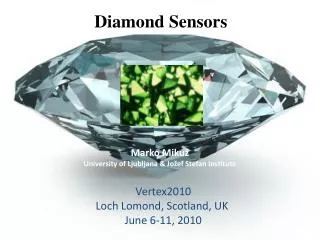
Diamond Sensorsfor High Energy Radiation and Particle Detection TIPP 2011 Chicago, IL, USA June 9-14, 2011 Marko Mikuž University of Ljubljana & JožefStefan Institute Ljubljana, Slovenia for the CERN RD-42 Collaboration
Outline • Diamond as sensor material • Radiation hardness: RD-42 • Diamond sensor applications • Radiation detection – beam monitors • ATLAS BCM/BLM • CMS BCM • Particle tracking • CMS PLT • ATLAS DBM Marko Mikuž: Diamond Sensors
Diamond as sensor material Marko Mikuž: Diamond Sensors
Sensor types - pCVD • Polycrystalline Chemical Vapour Deposition (pCVD) • Grown in μ-wave reactors on non-diamond substrate • Exist in Φ = 12 cm wafers, >2 mm thick • Small grains merging with growth • Grind off substrate side to improve quality → ~500-700 μm thick detectors Surface view of growth side Photo HK@OSU Side view Test dots on 1 cm grid Photograph courtesy of E6 Marko Mikuž: Diamond Sensors
Sensor types - scCVD • Single Crystal Chemical Vapour Deposition (scCVD) • Grown on HTHP diamond substrate • Exist in ~ 1 cm2 pieces, max 1.4 cm x 1.4 cm, thickness > 1 mm • A true single crystal • Fall-forward for sLHC pixel upgrade (single chips, wafers ?) • Needs significant improvement in size & price, ideas are around • After heavy irradiations properties similar to pCVD, headroom ~3x10¹⁵ p/cm2 • Recent commercial developments in adverse direction • Concentrate on max. ~5x5 mm2 pieces & packaging, main target market: dosimetry • Used on large scale in CMS PLT project ? Marko Mikuž: Diamond Sensors
Signal from CVD diamonds • No processing: put electrodes on, apply electric field • Surface preparation and metallization non-trivial ! • Trapping on grain boundaries (pCVD) and in bulk • Much like in heavily irradiated silicon • Parameterized with Charge Collection Distance, defined by • CCD = average distance e-h pairs move apart • Coincides with mean free path in infinite (t ≫ CCD) detector,CCD ~ t for scCVD mean not most probable CCD measured on recent 1.4 mm thick pCVDwafer from E6, and after thinning to 0.8 mm CCDvs. field for pCVD and scCVD diamond Marko Mikuž: Diamond Sensors
Radiation damage in diamond Charge multiplication • At extreme fluencescharge trapping the paramount radiation damage effect • Difference O(10) in x-section between charged/neutral traps • Filled (neutral) traps trap less (of the opposite carrier) • Basics of “pumping” • Egapin diamond 5 times larger than in Si • Many processes freeze out • Typical emission times order of months • Works also in Si at 300/5 = 60 K – “Lazarus effect” Marko Mikuž: Diamond Sensors
Radiation damage studies: RD-42 RD42 Collaboration 2011 100 participants from 32 institutes Marko Mikuž: Diamond Sensors
Irradiation: 24 GeV protons (PS) • For mean free path in infinite detector expect • With CCD0 initial trapping, ka damage constant • Larger CCD0performs better (larger collected charge) at any fluence • Can turn 1/ CCD0into effective “initial” fluence • expect CCD0~ ∞ for scCVD • pCVD and scCVD diamond follow the same damage curve • k ~ 0.7x10⁻¹⁸μm-1cm-2for PS (24 GeV) protons Test beam results Marko Mikuž: Diamond Sensors
Irradiation: 800 MeV protons (LANL) • Recent irradiations with 800 MeV protons at LANSCE Facility in Los Alamos, US • ~2x more damaging than PS protons k ~ 1.3x10⁻¹⁸μm-1cm-2 • Consistent with NIEL prediction • Work in progress, one more data point being analyzed Test beam results Marko Mikuž: Diamond Sensors
Irradiation: 70 MeV protons (Sendai) • Recent irradiations with 70 MeV protons at Cyric Facility in Sendai, Japan • 3x more damaging than PS protons k ~ 2x10-18μm-1cm-2 • NIEL prediction • factor of 6 • NIEL violation ?! • One more sample being analyzed Test beam results Marko Mikuž: Diamond Sensors
Irradiation: 25 MeV protons (KIT) • Recent irradiations with 25 MeV protons at Karlsruhe, Germany • 5x more damaging than PS protons k ~ 3.3x10⁻¹⁸μm-1cm-2 • NIEL prediction • factor of 15 • NIEL violation ! • Work in progress Source/test beam results Marko Mikuž: Diamond Sensors
NIEL/DPA calculations • NIEL calculations published by KIT group in Phys. Stat. Sol. • Protons • Ratio 800 MeV / 24 GeV: ~ 2 • Ratio 70 MeV / 24 GeV: ~ 6 ! • Ratio 25 MeV / 24 GeV: ~ 15 !! • Neutrons • 10 MeV n ~ 24 GeV p !! • Recent calculation by S. Mueller based on displacement per atom (DPA) value given by FLUKA (development version, preliminary) • Proton ratios: 1.2, 5, 10 (800, 70, 25MeV) • n(10 MeV)/p(24 GeV) ratio: 6 • NIEL not fully applicable to diamond W. de Boer et al. phys. stat. sol. (a) 204, No. 9 (2007)3009 Steffen Mueller - preliminary RD-42 meeting, April 2010 Marko Mikuž: Diamond Sensors
Damage constant from scCVD data • The radiation induced introduction of traps decrease the mean free path mfp • We measure CCD • CCD~mfpe+mfphin thick detectors t >> mfp, CCD • CCD degradation formula not applicable to scCVD since CCD0 = t; mfp0 →∞ • Relation CCD ↔ mfpfor homogeneous material • For lack of data assume mfpe = mfph • Comparison: • 24GeV p ksc= 0.9x10⁻¹⁸µm-1cm-2~ kpCVD = 0.7x10⁻¹⁸µm-1cm-2 • 25MeV p ksc= 3.0x10⁻¹⁸µm-1cm-2~ kpCVD= 3.3x10⁻¹⁸µm-1cm-2 • Work in progress, but looks quite good! CCD/t mfpe = mfph mfp = mfpe + mfph mfp/t Marko Mikuž: Diamond Sensors
scCVD irradiation at PSI • Single scCVD, d = 500 µm, irradiated with 200 MeVpions at PSI, Villigen, CH • Measured (source) CCD = 260 µm after 6.52x10¹⁴p/cm2 • Turns into mfp of 420 µm • k = 3.6x10⁻¹⁸ µm-1cm-2 • Appears high, but DPA peaks at 200 MeV (Δ) • Again, work in progress • Test-beam under way Steffen Mueller – priv. comm. Marko Mikuž: Diamond Sensors
Diamond sensor applications in HEP • All LHC exp’s use diamonds for beam monitoring & accident protection • Current and counting mode operation, TOF capability • O(100) diamond sensors employed • CMS is building Pixel Luminosity Telescope • 48 scCVD pixel modules (5 mm x 5 mm) • ATLAS is proposing Diamond Beam Monitor • 24 pCVD pixel modules (21 mm x 18 mm) • Upgrade plans include diamond as candidate for innermost pixel tracker layer(s) • Elaborate on four projects • Radiation monitoring: ATLAS BCM/BLM, CMS BCM/BCM-F • Particle detection: CMS PLT, ATLAS DBM Marko Mikuž: Diamond Sensors
ATLAS BCM/BLM TIPP talk by M. Fisher • BCM TOF concept • Collisions: in time • Background: out of time 3.5 m 1.9 m BLM 2 x 6 modules Measured TOF with beam BCM module BLM module 8x8 mm pCVD Marko Mikuž: Diamond Sensors
BCM performance BA is fired increasing activity PM buffer 1177 LHC orbits – ~100 ms ~10 ms after BA is fired the buffer is recorded for additional 100 LHC orbits (~10 ms) BCM AND BCM OR • Luminosity monitoring • 3564 hit maps for OR, ANDAC, XORA • Main ATLAS lumi monitor in 2011 • Insensitive to pile-up at high bunch lumi Marko Mikuž: Diamond Sensors • Dual threshold readout NINO • BA condition: 3/4L+3/4H on both sides • Beam dump fired by BCM during LHC aperture scan • Too sensitive at current conditions • Measures taken in 2011 to restore abort functionality, still passive • BLM - 12 diamonds read by machine BLM system (40 µs) provide beam protection • Active in beam abort system • Threshold set at conservative ID damage level Beam conditions monitoring
CMS Beam Condition Monitoring BCM1L BCM2 TIPP talk byM.E.CASTRO CARBALLO • 32 diamond detectors with standard LHC BLM readout. • Main purpose: Protection of Pixel and Tracker. Can assert beam dump if conditions are too bad. • Four positions for measurement: • BCM1L (Z=±1.8m), BCM2 (Z=±14.4m) • Different sensitivities of BCM2 and BCM1L to collision signal and background allow extraction of background from raw signal. • This fill with high background due to bad vacuum shows the calculation of background. • Detectors follow well the vacuum time structure • So far ... no conditions that would have triggered a beam dump • No failures of the system • No false beam aborts. Marko Mikuž: Diamond Sensors
CMS Fast Beam Conditions Monitor BCM1F Marko Mikuž: Diamond Sensors
CMS Pixel Luminosity Telescope • Dedicated, stand–alone luminosity monitor • Eight 3-plane telescopes each end of CMS • 1.60⁰ pointing angle r = 4.8 cm, z = 175 cm • Diamond pixel sensors active area: • 3.9 mm x 3.9 mm, scCVD diamond • Count 3-fold coincidences fast-or signals (40 MHz) • Full pixel readout pixel address, pulse height (1 kHz) • Stable 1% precision on bunch-by-bunch relative luminosity PLT plane Cassette for 12 planes Full cassette in test-beam Marko Mikuž: Diamond Sensors
PLT Production Status • 48 planes needed for PLT • will produce 60 planes Characterization • 32% rejected 23/73 • replaced by vendor • 11 remain to be characterized Plane assemblies • 77% pass 37/48 • double column loss after bump bonding • currently 37 good planes System and schedule • all components being delivered • final system test in July • plan to install during technical stop at beginning of 2012 Marko Mikuž: Diamond Sensors
Diamond pixel modules Module after bump bonding Complete module under test • Full modules built with I3 pixel chips @ OSU, IZM and Bonn C-sensor in carrier Pattern with In bumps Edgeless scCVD module pattern scCVD module Bump bonds Marko Mikuž: Diamond Sensors
Industrialization: 2nd full pixel pCVD module • 1st module to be built in industry • All steps from polished sensor to bump-bonding performed at IZM Berlin • Embedding in a ceramic wafer • Wafer scale metallization & UBM process • Removal from the ceramics • Backside metallization & cleaning • Flip chip Marko Mikuž: Diamond Sensors
ATLAS Diamond Beam Monitor • Proposed during last months as add-on to IBL • ATLAS decision expected soon • Contingent on pixel services replacement in 2013 • Spin-off from diamond bid for IBL • 24 diamond pixel modules arranged in 8 telescopes around interaction point • Bunch by bunch luminosity monitoring • Bunch by bunch beam spot monitoring • Installation in 2013 Marko Mikuž: Diamond Sensors
DBM first modules • Four DBM modules built at IZM • 21x18 mm2pCVD from DDL • FE-I4 ATLAS IBL pixel chip • 336x80 = 26880 channels, 50x250 μm2 • Largest ASIC/diamond flip chip assembly 4 modules after flip-chipping • X-ray perfect • Noise map uniform • Indication of success • Need source/test-beam to confirm Module on test board Diamond + I4 X-ray after bump bonding I4 only Noise map of a DBM module Marko Mikuž: Diamond Sensors
Applications in HEP: wrap-up Radiation monitors ATLAS DBM Particle trackers Marko Mikuž: Diamond Sensors
Summary • Recent progress in the diamond world • Improved understanding of radiation damage • Application in all LHC experiments • Building of pixel modules in industry • Diamond trackers under way ! Very interesting times for diamond in HEP ahead of us ! Marko Mikuž: Diamond Sensors