Download
1 / 15
150 likes | 397 Views
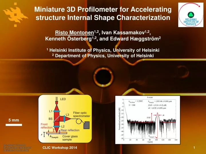
Risto Montonen 1,2 , Ivan Kassamakov 1,2 , Kenneth Österberg 1,2 , and Edward H ӕ ggström 2 1 Helsinki Institute of Physics, University of Helsinki 2 Department of Physics, University of Helsinki. Miniature 3D Profilometer for Accelerating structure Internal Shape Characterization. 5 mm.

E N D
Risto Montonen1,2, Ivan Kassamakov1,2,Kenneth Österberg1,2, and Edward Hӕggström2 1 Helsinki Institute of Physics, University of Helsinki2 Department of Physics, University of Helsinki Miniature 3D Profilometer for Accelerating structureInternal Shape Characterization 5 mm CLIC Workshop 2014
Introduction • Accelerating Structures (AS) comprising OFE Cu disks undergo permanent thermo-mechanical deformations during assembly [1,2,3] and RF operation [4,5]. • These deformations result in micron-level shape errors in AS. • > 10 mm axial depth rangewith sub-micron axialsensitivity is required. • Fourier Domain ShortCoherence Interferometry(FDSCI) -technique [7] Shape error Tolerance 1 µm [1,6] 5 µm [4] 140 µrad [1,6]
Design A: Setup • LED light source (L-793SRC-E, Kingbright) emits light with = 22 nm centered at = 654 nm. • Visible range fiber optic spectrometer (HR2000, Ocean Optics, Inc., spectral resolution = 0.44 nm) captures spectral interferogram constructed from front and rear reflections of the cover glass sample. • Modulation in the spectral interferogram reveals the sample thickness • Expect 160 µm axial depth range [7,8] • Cover glass samples with 3 different thicknesses (microscope #00, #0, and #1, () = 1.5205) Axial depthrange
Design A: Spectral interferogram processing [9] Interferogram processing Zeropadding Gaussian convolution kernel – equispaced sampling grid in F F-1 Gτ(F) Change of variable I(λ) I( f ) Interfero-gram Zeropadding g(t) Iτ(F) aτ(t) F-1 a(t) Change ofvariable A-scan a(r)
Design A: Spectral interferogram processing [9] Interferogram processing Zeropadding Gaussian convolution kernel – equispaced sampling grid in F F-1 Gτ(F) Change of variable I(λ) I( f ) Interfero-gram Zeropadding g(t) Iτ(F) aτ(t) Deconvolution F-1 a(t) Linearly sampled Iτ(F)obtained by convolving I( f ) with Gτ(F)– Fourier transforming is now allowed Change ofvariable A-scan a(r)
Design A: Spectral interferogram processing [9] Interferogram processing Zeropadding Gaussian convolution kernel – equispaced sampling grid in F F-1 Gτ(F) Change of variable I(λ) I( f ) Interfero-gram Zeropadding g(t) Iτ(F) aτ(t) F-1 a(t) Change ofvariable A-scan a(r)
Design A: A-scan analysis Axial sensitivity σh • Glass sample thickness hSample • Axial sensitivity σh • Signal to noise ratio SNR • -3 dB spreadingδr of the point spread function (PSF)
Design A: Setupverification Due to manufacturers delivery problems #00 data point is not measured yet • Erichsenmodell 497 • 1 µm resolution
Design A: Setup performance Expected appearance of #00 data points
Next step: Design B • Goal to reach the axial depth range across 10 mm • NIR LED (LED1550-35K42, Roithner Lasertechnik) + interferense filter (IF) (NIR01-1550/3-25, Semrock) = 8.8 nm centered at = 1550 nm • Tunable fiber Fabry-Perot (FFP) filter (FFP-TF2, Micron Optics) combined with photodetector (PD) (PT511-2, RoithnerLasertechnik) captures the spectral interferogram [10]. • 23.2 nm free spectral range (FSR) at = 1550 nm, = 0.025 nm • Expect 16.6 mm axial depth range [7,8]. • 1 – 10 mm quartz glass samples (() = 1.4440) [11]
Conclusions • Firstsetup towards Miniature 3D Profilometer -device works fine. • Proof of concept for sub-micron sensitivity metrology has been achieved. • Work to reach the requiredaxial depth range of 10 mm is currently ongoing. • Integration of the fiber optic probe and AS scanning systemare the followingsteps.
References [1] A Multi-TeV linear collider based on CLIC technology: CLIC Conceptual Design Report, edited by M. Aicheler, P. Burrows, M. Draper, T. Garvey, P. Lebrun, K. Peach, N. Phinney, H. Schmickler, D. Schulte, and N. Toge. [2] J.W. Wang, J.R. Lewandowski, J.W. Van Pelt, C. Yoneda, G. Riddone, D. Gudkov, T. Higo, T. Takatomi, Proceedings of IPAC’10, Kyoto, Japan, THPEA 064. [3] D.M. Owen, T.G. Langdon, Materials Science and Engineering A 216 (1996) 20-29. [4] H. Braun et al., CERN-OPEN-2008-021; CLIC-Note-764. [5] M. Aicheler, S. Sgobba, G. Arnau-Izquierdo, M. Taborelli, S. Calatroni, H. Neupert, W. Wuensch, International Journal of Fatigue 33 (2011) 396-402. [6] R. Zennaro, EUROTeV-Report-2008-081. [7]T-H. Tsai, C. Zhou, D.C. Adler, and J.G. Fujimoto, Optics Express 17 (2009) 21257-21270. [8] R.A. Leitgeb, W. Drexler, A. Unterhuber, B. Hermann, T. Bajraszewski, T. Le, A. Stingl, and A.F. Fercher, Optics Express 12 (2004) 2156-2165. [9] K.K.H. Chan and S. Tang, Biomedical Optics Express 1 (2010) 1309-1319. [10] J. Bailey, Atmospheric Measurement Techniques Discussions 6 (2013) 1067-1092. [11] I.H. Malitson, Journal of the Optical Society of America 55 (1965) 1205-1209.
Thank You CLIC Workshop 2014