Download
1 / 13
130 likes | 334 Views
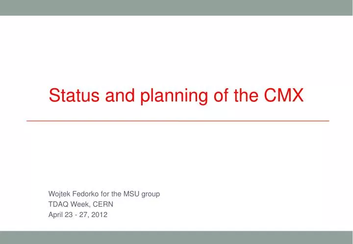
Status and planning of the CMX. Wojtek Fedorko for the MSU group TDAQ Week, CERN April 23 - 27, 2012. CMX: CMM upgrade. Will replace CMM: Backplane rate 40 → 160Mbs Crate to system rate (LVDS) 40 → 160Mbs Cluster information sent to Topological Processor (optical)

E N D
Status and planning of the CMX Wojtek Fedorko for the MSU group TDAQ Week, CERN April 23 - 27, 2012
CMX: CMM upgrade • Will replace CMM: • Backplane rate 40 →160Mbs • Crate to system rate (LVDS) 40 →160Mbs • Cluster information sent to Topological Processor (optical) • Optional partial TP functionality • Standalone TP is now planned • Some TP capability also designed onto the CMX W. Fedorko CMX status and plans
CMX: Use scenario with standalone TP Energy Jet Electron Tau Base- CMX FPGA Base- CMX FPGA Base- CMX FPGA Base- CMX FPGA Base- CMX FPGA Base- CMX FPGA Base- CMX FPGA Base- CMX FPGA Crate CMXs 12 LVDS Cables LVDS Cables LVDS Cables LVDS Cables - - - - - - - - System CMXs 1 x 12-fiber ribbon Base- CMX FPGA Base- CMX FPGA Base- CMX FPGA Base- CMX FPGA to CTP to CTP to CTP to CTP 12 x 12-fiber ribbons Optical Patch Panel Standalone Topological Processor to CTP N x 12 W. Fedorko CMX status and plans
The CMX overview ROI 2x G-Link Out VME-- VME-- Interface DAQ 3x 12-fiber ribbons IN TCM Interface 12x Optic IN TCM 6.4 Gbps inputs re-bundled from up to 12 Base-CMX TP-CMXFPGA Virtex-6 LX550T-FF1759 12x Optic IN Inputs from all JEM or CPM processors from this crate 12x Optic IN CTP output 2x33 LVDS pairs @ 40 Mbps (from TP-CMX via Base-CMX) 400 single ended @ 160Mbps Base-CMXFPGA Virtex-6 LX550T-FF1759 12x Optic OUT 6.4 Gbps outputs to Standalone TP and/or TP-CMX 2x 12-fiber ribbons OUT LVDS cables From Crate To System CMX 12x Optic OUT ROI 2x G-Link Out 3x27 LVDS pairs @ up to 160 Mbps DAQ W. Fedorko CMX status and plans
CMX: modular design, most cards assembled without TP functionality VME-- VME-- Interface TCM Interface TCM Inputs from all JEM or CPM processors from this crate CTP output 2x33 LVDS pairs @ 40 Mbps (System CMX only) 400 single ended @ 160Mbps Base-CMXFPGA Virtex-6 LX550T-FF1759 12x Optic OUT 6.4 Gbps outputs to Standalone TP and/or TP-CMX 2x 12-fiber ribbons OUT LVDS cables From Crate To System CMX 12x Optic OUT ROI 2x G-Link Out 3x27 LVDS pairs @ up to 160 Mbps DAQ W. Fedorko CMX status and plans
CMX development work on 3 fronts Engineering @MSU Philippe, Dan, and Chip CMX input module firmware @CERN Wojtek and Yuri VME/ACE/TTC (VAT) interface @CERN Yuri Request from Chris and David - to address and present: "The detailed timeline & schedule from now until completion of commissioning at Point 1 in 2014 and a set of milestones associated to this schedule - typically ~10, including details of review procedure" Initial CMX development schedule is still valid Minor adjustments W. Fedorko CMX status and plans
Initial CMX development schedule from 2011 2011: Project and engineering specifications CMX project Preliminary Design Review (Done) Preliminary design studies Test rig installed, checked out at MSU (postponed until 2012) 2012: Prototype design and fabrication CMX schematics and PCB layout Production Readiness Review Prototype fabrication, CMM firmware ported on CMX Basic tests for backward compatibility in test rig at MSU 2013: Prototype testing/installation/commissioning, final fabrication Full prototype tests in test rig at CERN CMX firmware development and test Test in the L1Calo system during shutdown Fabricate and assemble full set of CMX modules 2014: Final commissioning in the L1Calo trigger system in USA15 https://indico.cern.ch/getFile.py/access?contribId=31&sessionId=6&resId=0&materialId=slides&confId=152943 W. Fedorko CMX status and plans
2012 2012: Prototype design and fabrication CMX schematics and PCB layout CMX technology choice (FPGA choice, CMX/TP functionality) - DONE 6U VME test card for VAT interface – PCB ready for testing in June Real-time data path layout (ongoing) CMX input module firmware currently under test on the XILINX development module Power budget estimate Prototype fabrication mechanical testing in January Will happen within ~month, not urgent yet. Blank card, backplane connectors, front panel tests. CMM firmware ported on CMX Firmware for VAT interface (2 CPLD + TTC FPGA) to Spartan-3AN FPGA (Adapt VHDL code, create test bench, specify VME register model) (Yuri) Most of the work completed at Stockholm (PawelPlucinski, Sam Silverstein) Needs to be adapted to final package choice Basic tests for backward compatibility in test rig at MSU Production Readiness Review (L1Calo/TDAQ) Fall/Winter PRR after the prototype(s) is tested and final check before going into full production W. Fedorko CMX status and plans
2011/2012: design studies: Clock/parity recovery BUFR 96 bits @ 40MHz 40 MHz Clock/parity MMCM 40MHz register BUFIO Regional clock buffer (BUFR) x 16 80 MHz IDDR Data • Clock+Parity encoded on single line • Variable duty cycle • Setup: • Scheme tested using Virtex 6 eval board • Data capture developed, simulated and ‘Placed and Routed’ on target FPGA • Needs repeating – different package chosen W. Fedorko CMX status and plans
2012: PCB layout: VME/ACE/TTC (VAT) interface test card VME CPLD TTCrx TTC FPGA FC TTCDec TTC ACE CPLD SystemACE 5V0 • VME/ACE/TTC (VAT) part of CMM • Redesign HW with new components • Fit design into single device • 6U VME test card for • Hardware implementation • Main FPGA re-configuration • Software • To be merged into CMX design • PCB arrives in June • Next: • Firmware for VAT card • Firmware for Virtex 6 FPGA • Test Stand and software VME-- logic Spartan-3AN JTAG 1V2 3V3 2V5 Virtex6 CF 1V0 SystemACE 1V0 2V5 3V3 Connector for CANbus i/f Power W. Fedorko CMX status and plans
2012 PCB Layout: Backplane – FPGA connection NOT FINAL • Challenging milestone • Signal density • Avoid contention • Drives FPGA package choice • Implications for Firmware design W. Fedorko CMX status and plans
2013 2013: Prototype testing/installation/commissioning, final fabrication Full prototype tests in test rig at CERN Test in the L1Calo system during shutdown Fabricate and assemble full set of CMX modules W. Fedorko CMX status and plans
Conclusions • Schedule proposed is maintained • Minor adjustments • Tasks proceeding according to plan • Need more detailed set of steps for in-situ tests before and after first beam • Optimistic outlook for project completion W. Fedorko CMX status and plans