Download
1 / 17
180 likes | 322 Views
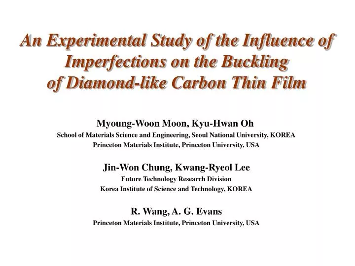
An Experimental Study of the Influence of Imperfections on the Buckling of Diamond-like Carbon Thin Film. Myoung-Woon Moon, Kyu-Hwan Oh School of Materials Science and Engineering, Seoul National University, KOREA Princeton Materials Institute, Princeton University, USA

E N D
An Experimental Study of the Influence of Imperfections on the Buckling of Diamond-like Carbon Thin Film Myoung-Woon Moon, Kyu-Hwan Oh School of Materials Science and Engineering, Seoul National University, KOREA Princeton Materials Institute, Princeton University, USA Jin-Won Chung, Kwang-Ryeol Lee Future Technology Research Division Korea Institute of Science and Technology, KOREA R. Wang, A. G. Evans Princeton Materials Institute, Princeton University, USA
Purpose and overviews • Purpose • The observation on the sources of interface imperfection • Defect, Free edge, Substrate Curvature • Optimization of imperfection instability • Overview • (Characterization of defect on the interface) - Surface profile on defect site: Atomic Force Microscopy - Cross sectioning of defect site : Focus Ion Beam - Chemical analysis for defect : Auger Electron Spectroscopy Observation for the condition of defect-induced delamination
Introduction of Interface delamination • General systems with Delamination or Buckle • -Highly compressed film • DLC or Diamond film on glass / Si • Gold on copper film on sapphire • Amorphous (hydrogenated ) Si film on glass/Si • Stainless steel on polycarbonate • Thermal Barrier Coatings system • Interface delamination on Diamond-Like Carbon film Imperfection deriven Delamination Buckle deriven Delamination
Imperfection I – Interface defects 4 mm 10 mm 10 mm 10 mm 10 mm 10 mm 20 mm The reflection of Small defects on the film surface after deposition Large defects
Imperfection II - Free edge Free edge 5 mm 50 mm 200 mm 10 mm Free edge effect on delamination Delamination sequence from free edge ( t = Real time) t=5 sec t=1 sec Thickness of film h= 0.13 mm h= 0.80 mm
Imperfection III – Substrate Curvature effect “Substrate curvature plays a role of imperfection” J. W. Hutchinson, JMPS, 49, 2001 L > 1 The condition of Preferred Propagation direction Concave : axial Convex : circumferential
Experiments on defect effects Deposition with CVD Diamond-like carbon films on glass substrates by PECVD with CH4 and C6H6 plus N2, Negative self bias voltage : -100 to -700V The film thickness : 0.13 ~ 0.46mm Residual compression : 1GPa and 3GPa resulting in telephone cord buckles. AFM In tapping mode (Digital Instrument company). Images of representative buckles and cross sectional profiles FIB Dual-Beam FIB (FEI Company, DB235). Direct cut along the buckle (damage free) To create the straight-sided buckle from telephone cord buckle. AES Auger Electron Spectroscopy Chemical analysis on several defect sites
Cross sections of defect sites - AFM Surface topology Profile of Cross section
Cross sectioning : small defect - FIB Defect Geometry Thickness of film h ~ 0.46mm Wavelength : 10 mm Amplitude : ~0.9 h Before cut After cut
Cross sectioning : Large defect - FIB Before cut After cut Defect Geometry Thickness of film h ~ 0.46mm Wavelength : 40 mm Amplitude : ~ 1.6 h Moon et al, Acta Mater., 2002
Chemical analysis underneath defect sites -AES 5 mm 10 mm Film surface (Refection of defect) Underneath film (Defect on substrate) - Auger electron spectroscopy-
Energy release rate with imperfection size The condition of Delamination propagation Hutchinson, He, Evans, 2000, JMPS
Summary of Observation on defect sites =1.9GPa E=90~100GPa Sub-critical No delamination Stationary Delamination only Super-critical Propagation of delamination . * Weiderhorn, S. M., J. Am. Ceram. Soc., 1967, 50, 407.
Summary • The source of imperfection on the interface • Defect, Free edge, and substrate curvature effect • The characterization of Defect • AFM :Measurement of Profile of defect on the film surface • FIB : Cross sectional analysis with fine • AES : Chemical analysis on foreign defect on the interface • The condition of Defect-induced delamination