Download
1 / 13
170 likes | 453 Views
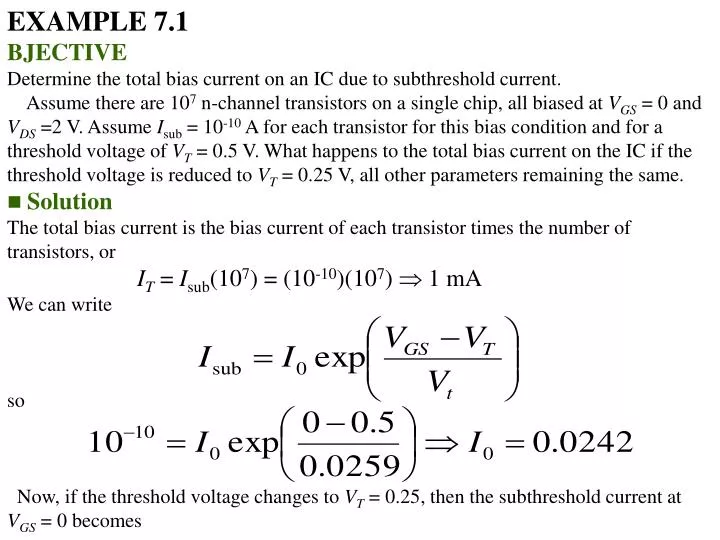
EXAMPLE 7.1 BJECTIVE Determine the total bias current on an IC due to subthreshold current.

E N D
EXAMPLE 7.1 • BJECTIVE • Determine the total bias current on an IC due to subthreshold current. • Assume there are 107 n-channel transistors on a single chip, all biased at VGS = 0 and VDS =2 V. Assume Isub = 10-10 A for each transistor for this bias condition and for a threshold voltage of VT = 0.5 V. What happens to the total bias current on the IC if the threshold voltage is reduced to VT = 0.25 V, all other parameters remaining the same. • Solution The total bias current is the bias current of each transistor times the number of transistors, or IT = Isub(107) = (10-10)(107) 1 mA We can write so Now, if the threshold voltage changes to VT = 0.25, then the subthreshold current at VGS = 0 becomes
or • Isub = 1.56 106 A • Now, the total bias current for this IC chip would be • IT = (1.56 10-6)(107) = 15.6 A • Comment • This example is intended to show that, taking into account subthreshold currents, the threshold voltage must be designed to be a “reasonable” value such that the zero-bias gate currents are not excessive.
EXAMPLE 7.2 • OBJECTIVE • To determine the effect of channel length modulation on the value of drain current. • Consider a n-channel MOSFET with a substrate impurity doping concentration of Na = 2 1016 cm-3, a threshold voltage of VT = 0.4 V, and a channel length of L = 1 m. The device is biased at VGS = 1 V and VDS = 2.5 V. • Solution We find that and VDS(sat) = VGS VT = 1 0.4 = 0.6 V Now or L = 0.181 m We can write or • Comment • Due to channel length modulation, the drain current is 22 percent larger than the ideal long channel value.
EXAMPLE 7.3 • OBJECTIVE • To calculate the effective electric field at threshold for a given semiconductor doping. • Consider a p-type silicon substrate at T = 300 K and doped Na = 3 1016 cm-3. • Solution From Equation (6.8b) in Chapter 6, we can calculat and which is xdT = 0.18 m. Then At the threshold inversion point, we may assume that Qn = 0, so the effective electric field from Equation (7.10) is found as • Comment • We can see, from Figure 7.10, that this value of effective transverse electric field at the surface is sufficient for the effective inversion charge mobility to be significantly less than the bulk semiconductor value.
EXAMPLE 7.4 • OBJECTIVE • To determine the ratio of drain current under the velocity saturation condition to the ideal long-channel value. • Assume an n-channel MOSFET with a channel length L = 0.8 m, a threshold voltage of VT = 0.5 V, an electron mobility of n = 700 cm2/V-s, and vsat = 5 106 cm/s. Assume that the transistor is biased at (a) VGS = 2 V and (b) VGS = 3 V. • Solution • We can write • For (a) VGS = 2 V, we find • and for (b) VGS = 3 V, we obtain • Comment • We see that as the applied gate-to-source voltage increases, the ratio decreases. This effect is a result of the velocity saturation current being a linear function of VGS VT , whereas the ideal long-channel current is a quadratic function of VGS VT .
EXAMPLE 7.5 • BJECTIVE • Calculate the threshold voltage shift due to short-channel effects. • Consider an n-channel MOSFET with Na = 5 1016 cm-3 and tox = 200 Å. Let L = 0.8 m and assume that rj = 0.4 m. • Solution We can determine the oxide capacitance to be and can calculate the potential as the maximum space charge width is found as
Finally, the threshold voltage shift, from Equation (7.22), is • or • VT = 0.101 V • Comment • If the threshold voltage of this n-channel MOSFET is to be VT = 0.40 V, for example, a shift of VT = 0.101 V due to short-channel effects is significant and needs to be taken into account in the design of this device.
EXAMPLE 7.6 • OBJECTIVE • Design the channel width that will limit the threshold shift because of narrow channel effects to a specified value.. • Consider a n-channel MOSFET with Na = 5 1016 cm-3 and tox = 200 Å. Let = / 2. Assume that we want to limit the threshold shift to VT = 0.1 V. • Solution From Example 7.5, we have From Equation (7.28), we can express the channel width as or W = 1.46 m • Comment • We can note that the threshold shift of VT = 0.1 V occurs at a channel width of W = 1.46 m, which is approximately 10 times larger than the induced space charge width xdT .
EXAMPLE 7.7 • BJECTIVE • Calculate the theoretical punch-through voltage assuming the abrupt junction approximation. • Consider an n-channel MOSFET with source and drain doping concentrations of Nd = 1019 cm-3 and a channel region doping of Na = 1016 cm-3. Assume a channel length of L = 1.2 m, and assume the source and body are at ground potential. • Solution The pn junction built-in potential barrier is given by The zero-biased source-substrate pn junction width is
The reverse-biased drain-substrate pn junction width is given by • At punch-through, we will have • Which fives xd = 0.864 m at the punch-through condition. We can then find • The punch-through voltage is then found as • VDS = 5.77 0.874 = 4.9 V • Comment • As the two space charge regions approach punch-through, the abrupt junction approximation is no longer a good assumption.
EXAMPLE 7.8 • BJECTIVE • Design the ion implant dose required to adjust the threshold voltage to a specified value. • Consider an n-channel MOSFET with a doping of Na = 5 1015 cm-3, and oxide thickness of tox = 500 Å, and an initial flat-band voltage of VFBO = 1.25 V. Determine the ion implantation dose such that a threshold voltage of VT = +0.70 V is obtained. • Solution We may calculate the necessary parameters as
The initial pre-implant threshold voltage is The threshold votage after implant, from Equation (7.31), is so that
Which gives • DI = 3.51 1011 cm2 • If the uniform step implant extends to a depth of xI = 0.15 m, for example, then the equivalent acceptor concentration at the surface is • or • Ns = 2.84 1016 cm3 • Comment • The required implant dose to achieve the desired threshold voltage is DI = 3.51 1011 cm-2. This calculation has assumed that the induced space charge width in the channel region is greater than the ion implant depth xI. We can show that this requirement is indeed satisfied in this example.