Download
1 / 41
420 likes | 707 Views
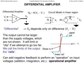
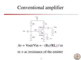
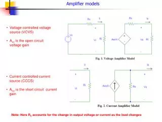
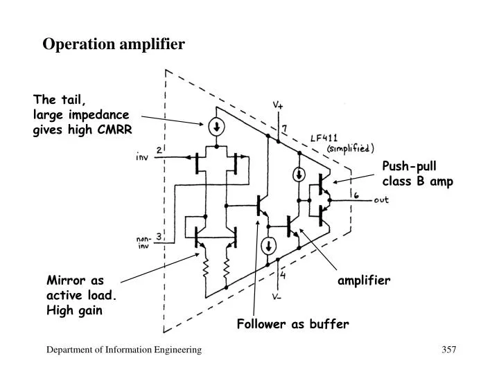
Operation amplifier. The tail, large impedance gives high CMRR. Push-pull class B amp. Mirror as active load. High gain. amplifier. Follower as buffer. Operational amplifier. Op-amp Differential amp + non-linear amp + output driver Op-amp has very high gain (A)

E N D
Operation amplifier The tail, large impedance gives high CMRR Push-pull class B amp Mirror as active load. High gain amplifier Follower as buffer
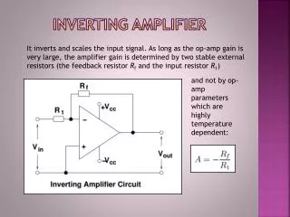
Operational amplifier • Op-amp • Differential amp + non-linear amp + output driver • Op-amp has very high gain (A) • But the gain is non-linear (because IC vs VBE is not linear) • Use global feedback to build linear amplifier • Exact value of the gain of the op amp is not important, as long as it is very large
Feedback Op amp golden rules Approximations: 1. Voltage difference between the two inputs is zero • Input draws no current Why? • VOUT = A VIN • If VOUT is around 10V, A=10,000, then VIN ~ 1mV, voltage difference ~ 1mV (close to zero) • FET draws virtually zero input current VIN VOUT
An easier method • Because A is so large that Ve ~ 0 (known as virtual earth) Ve ~ 0
Inverting amplifier • Input impedance (RIN)? • Ve ~ 0, so RIN = R1 • Important • gain is determined by external parameters that we can control (the resistors) • gain (A) of the op amp can be non-linear, its exact value is not important, as long as it is very large
Negative feedback • Feedback MUST be applied to the –ve terminal (–ve feedback), so that Ve ~ 0 (IMPORTANT) B) Doesn’t Work A) Works
Positive feedback • +ve VIN produces large +ve VOUT • +ve VOUT produces +ve Ve • which produces an even larger +ve output. • output reaches max +ve supply voltage very quickly • useless as an amplifier (but good as a switch, small +ve signal produces large maximum output)
Non-inverting amplifier • RIN? • infinite ! • V-? • V- ~ VIN (Ve ~ 0) • Current through R1? • I=VIN / R1 • Output voltage? Ve V-
Voltage follower • Left side circuit (work) • If output is too large, then feedback to the –ve terminal will reduce output to a equilibrium level until Ve ~ 0 • Right side circuit (doesn’t work) • If output is too large, then feedback to the +ve terminal will make the output even larger until saturation
Power booster • The output current of an op amp is usually small • If you want larger output current, add an external push-pull follower made of discrete power transistors
Power booster • Normally push-pull follower has cross-over distortion • Not this one ! • The gain of the amplifier depends on the external feedback circuit • The forward gain of the internal circuit can be non-linear but must be large
Power of feedback • Can put in anything in the forward loop, still get good result
Funny circuits • What is the function of this circuit?
Funny circuits • Does this circuit work?
Practical circuits • Design an inverting amplifier with a gain of -100, to be driven by a source whose output impedance is 1MW • What is the value of R? How about 100R?
Practical circuits • A better solution
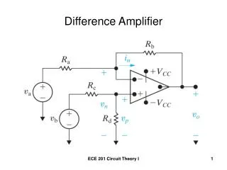
Practical circuits • Summing circuit (an adder) VIN VOUT
V1 V2 I V3
Practical circuits (a simple digital-to-analog converter) • VOUT = A+2B-3C
Practical circuits • Perfect current source using imperfect FET V+-VIN
Active rectifier • The simple passive rectifier has 0.6V drop between input and output
Active rectifier without the diode drop (optional) • The active rectifier does not have the 0.6V drop !! • VIN >0, VOUT is +ve, diode is short-circuit • Feedback => VOUT = VIN (no 0.6V DC offset)
Problem • –ve input to V+, VOUT , diode is open circuit • VOUT pushes to –ve extreme • When input becomes +ve, takes a long time for the output to move from –ve to +ve (limited by the slew rate)
Active rectifier (optional) • This improved circuit prevents the rectifier from saturation
Negative-impedance converter (NIC) • An interesting two-terminals active device • apply a +ve voltage, you see a current flowing OUT • a negative impedance (!!) • i.e. ZIN = - Z !! • (leave the proof as exercise)
Gyrator • The following circuit is a gyrator • (leave the proof as exercise)
Gyrator • Use of gyrator • can turn a capacitor into inductor !! • How? • ZIN behaves as an inductor with L = CR2 • The use • replace bulky inductors by small gyrated capacitors • useful in integrated circuit design and small devices
Positive feedback • Apply feedback to the non-inverting (+ve) terminal • small +ve input produces a larger +ve output • output is feedback to the non-inverting input • produces an even larger output • quickly push the output to saturation • Uses • Comparators • Oscillators
Comparator – a simple switch • Output = +15V if VIN < 0 • Output = -15V if VIN > 0 +15V VIN - + VOUT -15V
A poor comparator because • if the input is noisy, the output makes several transitions (switching noise)
311 op amp • The output stage (emitter follower) is connected to external power supply • User can choose the output voltage they like
Schmitt trigger (an inverter switch, high VIN, low VOUT) • Hysteresis (circuit has memory) • the output switches at two separate threshold
Analysis • If VOUT = high (~5V) • VOUT ~= 5V, • Switching threshold V+ = 5V • When VIN > 5V • VOUT =0V • Switching threshold V+=4.76V • Now if VIN drops slightly below 5V • VOUT won’t change state • Eliminate noisy switching
Analysis • VIN > 5V, VOUT=0V, V+ =4.76V • If VIN < 4.76V, VOUT=5V, • V+ =5V (the new threshold)
Positive feedback • if phase shift = 180o in box ‘X’ at certain frequency, then the feedback becomes +ve (unstable) !! • This high frequency has sustained itself even there is no input • oscillation
Nasty oscillators • A follower driving a long cable (a common problem) • phase shift through the op amp = 180o • cable’s capacitance adds another 90o • The internal capacitance at high frequency adds another 90o • The follower oscillates ! (cable capacitance)
Ways to break the oscillation • Op amp oscillates at high frequency because of the additional phase shift introduced by its internal capacitor • Solution • Reduce the loop gain AB at high frequency • At the frequency that may cause oscillation, make A ~ 0, so that the loop gain (AB) < 1 • Op am that does this is called frequency compensated op amp • Disadvantage is that the max bandwidth is reduced
One oscillates, the other not • 411 is frequency compensated, never oscillates 411 311 May oscillates Never oscillates |A| |A| f f focc
Slew rate • The rate that output can change • Wider bandwidth -> higher frequency -> faster slew rate • 311 has faster slew rate, good as a switch