Download

1 / 17
180 likes | 304 Views
Study on Reducing Thermal Properties of M-DHBT. 2005. 6. 16 설경선. INDEX. Introduction Trend Overview of HBT Overview of Double HBT Overview of Metamorphic HBT Key issues of M-HBT (Self-Heating) Thermal resistance comparison M-HBT vs InP L-HBT

E N D
Study on Reducing Thermal Properties of M-DHBT 2005. 6. 16 설경선
INDEX • Introduction • Trend • Overview of HBT • Overview of Double HBT • Overview of Metamorphic HBT • Key issues of M-HBT (Self-Heating) • Thermal resistance comparison • M-HBT vs InP L-HBT • M-HBT with graded InAlP buffer vs InP buffer • Thermal resistance of InP-Based MHBT on GaAs subs using grade InxGa1-xP • Conclusion • Reference
Introduction (Trend) • Trend for GaAs Semiconductors in Handsets • Demand on GaAs is driven by handset industry • Power amp / switch / small signal amp • GaAs covers 90% of Power amp market WHY? • Demand for high efficiency / output power at low(3V) supply voltage HBT / MESFET amp • HBT : require single polarity power supply • Better amplifier linearity Fig. PA market share estimate by semiconductor technology for 2004 (source: RFMD)
Introduction (Overview of HBT) • Merits • Wide bandgap emitter high base dopping base resistance↓, device speed↑ • Low emitter-base turn on voltage reduce in power consumption • Electron transit time (factor of epitaxial growth, not lithography) • Entire emitter area conducts current flow high current handling per unit area • Low 1/f noise
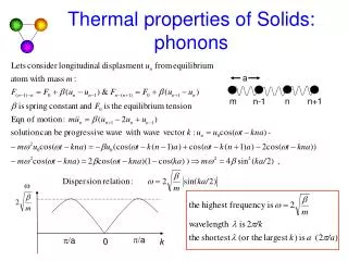
Introduction (Double HBT) • Double Heterojunction (increased collector bandgap) • Suppress in hole injection into base from collector (when B-C junction forward biased) • Diminish in charge storage in saturation • Speed up device turn-off from saturation region • Symmetrical (circuit flexibility) • Increase in BV • Reduction in leakage current Fig. Energy-bandgap diagram of DHBT
Metamorphic low cost Good performance Overview of Metamorphic HBT • InP based HBT • Superior material transport properties (>SiGe, GaAs) • ft / fmax / Je • Higher Thermal conductivity : GaAs(0.55W/cm-℃), InP(0.68W/cm-℃) • Problem : Cost, mechanical property (fragile) • Metamorphic HBT grown on GaAs substrate • GaAs substrate + InP HBT Epitaxy • Use of Buffer • ( ex) InAlAs / InAlP / InP / AlGaAsSb)
Key issues of HBT (Self-Heating). • Self-Heating effect • Negative slope : due to self heating increase in IB & IC(Δ IB > Δ IC) • Negative resistance effect becomes significant when power dissipation is large Fig. IC vs VCE
InGaAs 200nm n-type 2E19 InGaAs 200nm n-type 2E19 InAlAs 250nm n-type 5E18 InAlAs 250nm n-type 5E18 InAlAs 100nm n-type 4E17 InAlAs 100nm n-type 4E17 InGaAs 50nm p-type 4E19 InGaAs 50nm p-type 4E19 InGaAs 40nm n-type 1E16 InGaAs 40nm n-type 1E16 InGaAs 7nm p-type 1E18 InGaAs 7nm p-type 1E18 InP 7nm n-type 1E18 InP 7nm n-type 1E18 InP 390nm n-type 1E16 InP 390nm n-type 1E16 InGaAs 30nm n-type 8E18 InGaAs 30nm n-type 8E18 InP 550nm n-type 8E18 InP Substrate Metamorphic Buffer InxAl1-xAs GaAs S.I Substrate Layer structure of MHBT on GaAs Layer structure of InP LHBT Thermal resistance comparison 1. • Comparison of M-HBT & InP L-HBT
Thermal resistance comparison 1. VBE vs VCE at 50℃ Common emitter I-V • MHBT show • -Slightly lower offset voltage • Relatively lower current gain • Higher thermal resistance Rth at range of 30~150℃
Thermal resistance comparison 2. • Comparison of M-DHBT with graded InAlP buffer & InP • High speed DHBT must operate at Emitter power density exceeding 250 kW/cm2 • Thermal resistance is critically dependent of subcollector / buffer / substrate • Why InAlP : Thermally advantageous relative to InAlAs buffer • Why InP : comparable thermal conductivity to InP-LHBT
Thermal resistance comparison 2. • Comparison of M-HBT with graded InAlP buffer & InP • upper buffer thermal conductivity is more important (heat flux spread) • InxAl1-xP(x=1 at upper buffer, x=0.5 at lower buffer) • advantageous relative to AlGaAsSb & InAlAs buffer (InAs-AlAs & AlGaAs-AlGaSb : upper buffer has low thermal conductivity)
Thermal resistance comparison 2. Layer structure of MDHBT DC parameter of InP & InAlP buffer layer Temperature rise at 7.5mW disspation bias
Thermal resistance comparison 3. • Thermal resistance of InP-Based MHBT on GaAs subs using grade InxGa1-xP • Problem of direct growth of InP on GaAs subs : • high surface roughness / defect density of buffer layer • Graded InxGa1-xP buffer • Upper buffer(x=1, InP) (0.68W/cm-K) • In0.5Ga0.5P(~0.16W/cm-K) > In0.53Ga0.47As(0.044W/cm-K)
Thermal resistance comparison 3. Layer structure of MDHBT DC parameter of InP & InAlP buffer layer
Thermal resistance comparison 3. Common emitter I-V VBE vs VCE at 50℃ Rth at range of 30~150℃
Conclusion • InP buffer : advantageous reduction on thermal resistance • InGaP buffer : improve in material quality A: LHBT B: MHBT with InGaP buffer C: MHBT with InAlAs buffer
Reference • On the Thermal Resistance of Metamorphic and Lattice-Matched InP HBTs: A Comparative Study Hong Wang, Hong Yang, K. Radhakrishnan and Chee Leong Tan • Thermal Properties of Metamorphic Buffer Materials for Growth of InP Double Heterojunction Bipolar Transistors on GaAs Substrates Y. M. Kim, M. Dahlstrom, M. J. W. Rodwell, and A. C. Gossard 2003 • Thermal stability of current gain in InGaP/GaAsSb/GaAs double-heterojunction bipolar ransistors B. P. Yan, C. C. Hsu, X. Q. Wang, and E. S. Yang 2004 • Thermal Resistance of Metamorphic InP-Based HBTs on GaAs Substrates Using a Linearly Graded InxGa1 xP Metamorphic Buffer Hong Yang, Hong Wang, Member, IEEE, K. Radhakrishnan, Member, IEEE, and Chee Leong Tan 2004 • Trends and Opportunities for Gallium Arsenide Semiconductors in Handsets Paul J. Augustine • Low Leakage and High Speed InP/In0.53Ga0.47As/InP Metamorphic HBT on GaAs substrate Y.M.Kim, M.J.W. Rodwell, A.C. Gossard • InGaAs-InP Metamorphic DHBTs Grown on GaAs With Lattice-Matched Device Performance and ft, fmax >268Ghz Zach Griffith, YoungMin Kim, Mattias Dahlstrom 2004