Download
1 / 23
230 likes | 317 Views
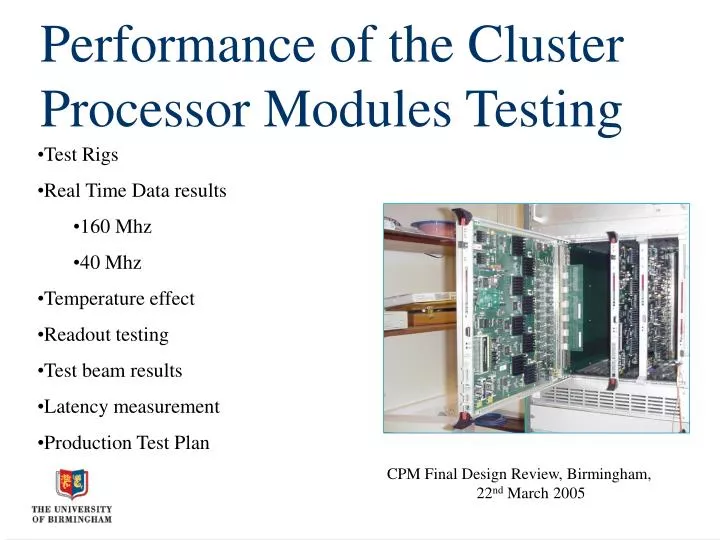
Performance of the Cluster Processor Modules Testing. Test Rigs Real Time Data results 160 Mhz 40 Mhz Temperature effect Readout testing Test beam results Latency measurement Production Test Plan. CPM Final Design Review, Birmingham, 22 nd March 2005. Cluster Processor Module: Test.

E N D
Performance of the Cluster Processor Modules Testing • Test Rigs • Real Time Data results • 160 Mhz • 40 Mhz • Temperature effect • Readout testing • Test beam results • Latency measurement • Production Test Plan CPM Final Design Review, Birmingham, 22nd March 2005
Cluster Processor Module: Test • Two kinds of test • Real Time Data • LVDS Rx (80 Chips) • Serialisers (20 Chips) • Cp Chip (8 Chips) • Hit Results (2 chips) • Asynchronous Data • DAQ (1 chip) • RoI (1 chip)
Cluster Processor Modules: Test Rigs • Thorough Tests were made with real or emulated module: • Downstream module was • Emulated: One LVDS Source Module (LSM), designed to emulate Preprocessor Module • Upstream Module were • Emulated: Glink Rx where Glink output where dump into big RAMs • Real: • Common Merger Module • ROD • One CPM was integrated with real modules during the CERN Test Beam in Oct04
Test Vectors Cluster Processor Module: Testing Process • Parameter • Clock delay • L1A rate • … Unit Under Test H/W Data Spy RAM Playback Memory • Data type: • physics • ramp • crosstalk • … Errors Files + - errors Simulation Sim Data parameter
Cluster Processor Modules: Test Rigs • Thorough Tests were made with real or emulated module: • Downstream module was • Emulated: One LVDS Source Module (LSM), designed to emulate Preprocessor Module • Upstream Module were • Emulated: Glink Rx where Glink output where dump into big RAMs • Real: • Common Merger Module • ROD • One CPM was integrated with real modules during the CERN Test Beam in Oct04
Cluster Processor Module: LVDS Data Results - 1 deskew1 • Source of data : Lvds Source Module • Data at the input of the serialisers are strobed at 40 MHz with Deskew1 • TTCvi/TTCex system was used to send the clock • The serialiser chip clock was changed via the I2C port of TTCrx • Timing window measured by delaying input serialiser chip clock in 104 ps steps • Error free zone of 20 ns Srl RAM DLL 20 ns
Cluster Processor Module: LVDS Data Results - 2 Each individual serialiser show a transition less than 2 ns Spread of tracks length expand it up to 5 ns Bit Error Rate Test performed at the input of the serialiser chip: < 10-13 per channel with pseudo random data (modified Serialiser F/W used)
Cluster Processor Module: Real Time Data deskew2 • Serialiser playback memories or LSM were used to drive data up to the CP chips • Delay between CP chip clock (deskew2) and SRL chip clock (deskew1) was varied • Delay was added using the available 104 ps step sizes deskew1 CP DLL Srl RAM DLL Srl RAM DLL CP DLL Srl RAM DLL
Cluster Processor Module: Real Time Data • Two F/Ws for the CP chips exist • One for debugging purpose: capture data on each individual pin (108) • One with the cluster algorithm, ATLAS version • Tests consisted of • Aligned clocks of different board with an oscilloscope • Load F/W with debugging mode • Perform a TTC scan • Record data error profile of each input pin • Load F/W with algorithm • Perform TTC scan • Record RoI profile of each CP chip • Record Parity error profile of each CP chip
Cluster Processor Module: Real Time Data: Data Error Profile • TTC scan using debugging mode • One 2nd CPM on the right-hand side (dashed profile) • Scan is performed over 25 ns, but input data run at 160 MHz: pattern of 6.25 ns period observed • Data Error free timing window around 2.5 ns 2.5 ns
Cluster Processor Module: Real Time Data • Timing window on each individual pin is around 4 ns • Reduce to 2.5 ns due to spread of track length • Two clocks phases are provided to capture on-board and backplane data After Correction Before Correction
Cluster Processor Module: Real Time Data • Overall Spread over 1 CPM Before Correction After Correction
Cluster Processor Module: Real Time Data • F/W with algorithm was used • RoI correctly processed • Parity Error profiles with a CPM either on the Left- or -Right Handside are correctly aligned • A total window of 2 ns is measured 2nd CPM on Left 2nd CPM on Right
Cluster Processor Module: Real Time Data: Temperature Effect • One CPM was put in an oven, remotely control trough a VME cable link to a CPU • The temperature was ranged from 5oC to 50oC • TTC scan of only on-board data was performed • Over that period, a shift of 500 ps has been measured • Reduced the data error free window to 1.5 ns
Cluster Processor Module: Hit multiplicities output • Multiplicities of different thresholds are calculated in real time at the output of the Hit Merger chip • Multiplicities are transmitted via the backplane to the CMM • Hit data were recovered inside the spy memory of the CMM • Timing scan was performed by delaying serialiser chip clock • Error free timing window of 12 ns, the rest of the period spent to calculate the multiplicities
Cluster Processor Module: Readout Frame Definition RoIs found by the CP are stored in a FIFO and sent to a ROD with a Bunch Crossing Number (BCN) attached on each L1A DAQ monitoring data, consisting of energies from 80 TT as well as resulting hit multiplicities are also sent to a ROD on each L1A. Data from up to 5 consecutive bunch crossings can be sent Parity BCN (h,f) Control Flag Threshold passed TT4-7 TT0-3 Parity HIT/BCN TT79-76 TT4-7 TT0-3
Cluster Processor Module: Readout Testing Setup • DSS used as a source of L1A pulses with a known pattern • No and rate of L1A controlled • TTCvi/TTCex system used with external input signals • Simulation data were generated according to known occurrence of L1As • Error checks were performed • At B’ham: on spy memory inside a ROD emulator (Glink Rx), on BCN and Data value • At RAL: using PC ROS where data were compared event per event basis with the simulation
Cluster Processor Module: Readout Testing Results • Burst rates of L1A up to 130 kHz were tested for Slice DAQ and RoI with no errors • DAQ frame with the minimal required separation of 5 ticks between L1As were recovered successfully • Up to 5 consecutive BCs DAQ data per event were also transmitted error free • Runs of up to more than 1h were performed showing no error
Cluster Processor Module: Test Beam Results • The CPM was integrated with • 2 CMMs • 1 PPMs • 2 RODs • Data correctly received by the CPM • Use of CPM DAQ to look at digitized calorimeter pulse over 5 time-slice • Data analysis of the test beam shows algorithm perform as expected
Cluster Processor Module: Latency measurement: old F/W version 50 ns .5 tck 13.4 ticks 2 ticks 2.5 ticks 8.4 ticks Lvds Rx Serialiser CP Chip Hit
Cluster Processor Module: Latency Saving • The serialiser chip was having an extra 12 ns: • Remove … • …but 6.25 ns added to cope with clock alignment scheme • The CP chip old version was having an obsolete calibration scheme and extra F/Fs on real time path • By removing them, 2 ticks have been saved • Not re-measured since but the offset of the readout has to be moved back by 2 ticks • Hit • No change, but if decide to clock the output with deskew1, ½ tick will be added 2.2 BC (-.25) 6.4 BC (-2.) .5 BC
Cluster Processor Module: Latency measurement • The total estimate latency for the CP is of 11.2 BC • The estimation of the latency from the test beam measurement is of 82 BC, but without a CPM in the chain, only JEM and looking at total energy • The latency of the CMM, part of the CP, was roughly measured of 4.9, and of the JEM 8.9 BC = 13.8 BC • Applied to the CPM 11.2+4.9, CP latency = 16.1 BC • The total L1A latency might exceed by 2 ticks, but still inside the 20 BC contingency.
LSMs CPM Production Plan CPM CPM CPM CPM CMM CMM • Test Rigs: • To test up to 2 CPMs in parallel • Use of present Online ATLAS Software to go trough the following set of tests • Testing LVDS Rx with LSM • Perform TTCscan with data, check connectivity • Load serialiser with F/W dedicated for BER • Perform TTC scan for BER profile • Load CP Chip with debugging feature • Perform TTC scan on data, measure and record timing window • Load CP Chip with algorithm • Perform TTCscan • Record data and parity error profile • Record hit merger data error profile from CMM • Overnight run looking at DAQ/RoI parity error • Production plan • 2 CPMs a day (with overnight run) • 65 CPMs-> test done in less than 2 months • Set of histograms comes with each CPMs