Download
1 / 31
310 likes | 438 Views
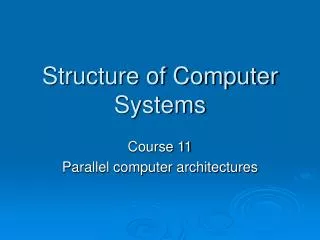
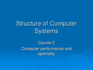
Computer Structure PC Structure and Peripherals. Lihu Rappoport and Adi Yoaz. Hard Disks. Platters. Hard Disk Structure. Rotating platters coated with a magnetic surface Each platter is divided to tracks: concentric circles Each track is divided to sectors

E N D
Computer StructurePC Structure and Peripherals Lihu Rappoport and Adi Yoaz
Platters Hard Disk Structure • Rotating platters coated with a magnetic surface • Each platter is divided to tracks: concentric circles • Each track is divided to sectors • Smallest unit that can be read or written • Disk outer tracks have more space for sectors than the inner tracks • Constant bit density: record more sectors on the outer tracks • speed varies with track location • Moveable read/write head • Radial movement to access all tracks • Platter rotation to access all sectors • Buffer Cache • A temporary data storage area used to enhance drive performance Sector Track
Disk Access • Seek: position the head over the proper track • Average: Sum of the time for all possible seek / total # of possible seeks • Due to locality of disk reference, actual average seek is shorter: 4 to 12 ms • Rotational latency: wait for desired sector to rotate under head • The faster the drives spins, the shorter the rotational latency time • Most disks rotate at 5,400 to 15,000 RPM • At 7200 RPM: 8 ms per revolution • An average latency to the desired information is halfway around the disk • At 7200 RPM: 4 ms • Transfer block: read/write the data • Transfer time is a function of: sector size, rotation speed, and recording density: bits per inch on a track • Typical values: 100 MB / sec • Disk Access Time = Seek time + Rotational Latency + Transfer time + Controller Time + Queuing Delay
EIDE Disk Interface • EIDE, PATA, UltraATA, ATA 100, ATAPI: all the same interface • Uses for connecting hard disk drives and CD/DVD drives • 80-pin cable, 40-pin dual header connector • 100 MB/s • EIDE controller integrated with the motherboard • EIDE controller has two channels • Primary and a secondary, which work independently • Two devices per channel: master and slave, but equal • The 2 devices take turns in controlling the bus • If there are two device on the system (e.g., a hard disk and a CD/DVD) • It is better to put them on different channels • Avoid mixing slower (DVD) and faster devices (HDD) on the same channel • If doing a lot of copying from drive to drive • Better performance by separating devices to separate channels
Disk Interface – Serial ATA (SATA) • Point-to-point connection • Dedicated BW per device (no sharing) • No master/slave jumper configuration needed when a adding a 2nd SATA drive • Increased BW • SATA rev 1: 150 MB/sec • SATA rev 2: 300 MB/sec • SATA rev 3: 600 MB/sec • Thinner (7 wires), flexible, longer cables • Easier routing, easier installation, better reliability, improved airflow • 1/6 the board area compared to EIDE connector • 4 wires for signaling + 3 ground to minimize impedance and crosstalk • Current HDDs still do not utilize SATA rev 3 BW • HDD peak (not sustained) gets to 157 MB/s • SSD gets to 250 MB/sec
Flash Memory • Flash is a non-volatile, rewritable memory • NOR Flash • Supports per-byte data read and write (random access) • Erasing (setting all the bits) done only at block granularity (64-128KB) • Writing (clearing a bit) can be done at byte granularity • Suitable for storing code (e.g. BIOS, cell phone firmware) • NAND Flash • Supports page-mode read and write (0.5KB – 4KB per page) • Erasing (setting all the bits) done only at block granularity (64-128KB) • Suitable for storing large data (e.g. pictures, songs) • Similar to other secondary data storage devices • Reduced erase and write times • Greater storage density and lower cost per bit
Flash Memory Principles of Operation • Information is stored in an array of memory cells • In single-level cell (SLC) devices, each cell stores one bit • Multi-level cell (MLC) devices store multiple bits per cell using multiple levels of electrical charge • Each memory cell is made from a floating-gate transistor • Resembles a standard MOSFET, with two gates instead of one • A control gate (CG), as in other MOS transistors, placed on top • A floating gate (FG), interposed between the CG and the MOSFET channel • The FG is insulated all around by an oxide layer electrons placed on it are trapped • Under normal conditions, will not discharge for many years • When the FG holds a charge, it partially cancels the electric field from the CG • Modifies the cell’s threshold voltage (VT): more voltage has to be applied to the CG to make the channel conduct • Read-out: apply a voltage intermediate between the possible threshold voltages to the CG • Test the channel's conductivity by sensing the current flow through the channel • In a MLC device, sense the amount of current flow
Flash Write Endurance • Typical number of write cycles • Bad block management (BBM) • Performed by the device driver software, or by a HW controller • E.g., SD cards include a HW controller perform BBM and wear leveling • Map logical block to physical block • Mapping tables stored in dedicated flash blocks or • Each block checked at power-up to create a bad block map in RAM • Each write is verified, and block is remapped in case of write failure • Memory capacity gradually shrinks as more blocks are marked as bad • ECC compensates for bits that spontaneously fail • 22 (24) bits of ECC code correct a one bit error in 2048 (4096) data bits • If ECC cannot correct the error during read, it may still detect the error
Flash Write Endurance (cont) • Wear-leveling algorithms • Evenly distribute data across flash memory and move data around • Prevent from one portion to wear out faster than another • SSD's controller keeps a record of where data is set down on the drive as it is relocated from one portion to another • Dynamic wear leveling • Map Logical Block Addresses (LBAs) to physical Flash memory addresses • Each time a block of data is written, it is written to a new location • Link the new block • Mark original physical block as invalid data • Blocks that never get written remain in the same location • Static wear leveling • Periodically move blocks which are not written • Allow these low usage cells be used by other data
Solid State Drive – SSD • Most manufacturers use "burst rate" for Performance numbers • Not its steady state or average read rate • Any write operation requires an erase followed by the write • When SSD is new, NAND flash memory is pre-erased • Consumer-grade multi-level cell (MLC) • Allows ≥2 bit per flash memory cell • Sustains 2,000 to 10,000 write cycles • Notably less expensive than SLC drives • Enterprise-class single-level cell (SLC) • Allows 1 bit per flash memory cell • Lasts 10× write cycles of an MLC • The more write/erase cycle the shorter the drive's lifespan • Use wear-leveling algorithms to evenly distribute writes • DRAM cache to buffer data writes to reduce number of write/erase cycles • Extra memory cells to be used when blocks of flash memory wear out
SSD (cont.) • Data in NAND flash memory organized in fixed size in blocks • When any portion of the data on the drive is changed • Mark block for deletion in preparation for the new data • Read current data on the block • Redistribute the old data • Lay down the new data in the old block • Old data is rewritten back • Typical write amplification is 15 to 20 • For every 1MB of data written to the drive, 15MB to 20MBs of space is actually needed • Using write combining reduces write amplification to ~10% • Flash drives compared to HD drives: • Smaller size, faster, lighter, noiseless, lower power • Withstanding shocks up to 2000 Gs (like 10 foot drop onto concrete) • More expensive (cost/byte): ~2$/1GB vs ~0.1$/1GB in HDD
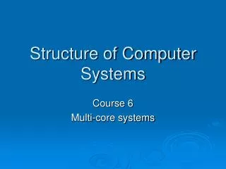
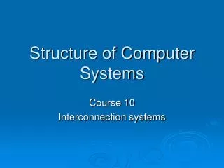
Computer System Structure – 2009 External Graphics Card HDMI PCI express ×16 North Bridge (GMCH) CPU BUS DDRII Channel 1 LLC On-board Graphics Memory controller Core Mem BUS DDRII Channel 2 Core IO Controller South Bridge (ICH) PCI express ×1 USB controller IDE controller SATA controller PCI Lan Adap Sound Card Floppy Drive keybrd mouse Old DVD Drive Hard Disk Parallel Port Serial Port speakers LAN
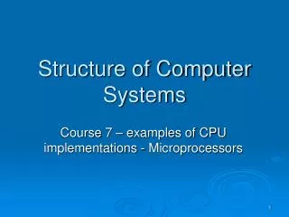
Computer System – Nehalem External Graphics Card PCI express ×16 North Bridge DDRIII Channel 1 CPU BUS Cache Memory controller On-board Graphics Mem BUS HDMI Core DDRIII Channel 2 Core IO Controller South Bridge PCI express ×1 USB controller SATA controller SATA controller PCI Lan Adap Sound Card Floppy Drive keybrd mouse DVD Drive Hard Disk Parallel Port Serial Port speakers LAN
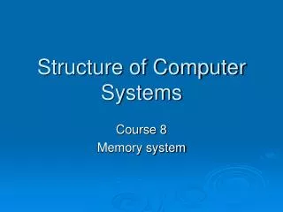
Computer System – Sandy Bridge External Graphics Card PCI express ×16 2133-1066 MHz DDRIII Channel 1 Memory controller Cache GFX System Agent Mem BUS Core DDRIII Channel 2 Core Display link 4×DMI Line out Audio Codec Display port South Bridge (PCH) Line in S/PDIF out HDMI S/PDIF in DVI exp slots D-sub BIOS PCI express ×1 LPC Super I/O Lan Adap SATA USB SATA Parallel Port Floppy Drive PS/2keybrd/mouse mouse DVD Drive Hard Disk Serial Port LAN
PCH Connections • LPC (Low Pin Count) Bus • Supports legacy, low BW I/O devices • Typically integrated in a Super I/O chip • Serial and parallel ports, keyboard, mouse, floppy disk controller • Other: Trusted Platform Module (TPM), Boot ROM • Direct Media Interface (DMI) • The link between an Intel north bridge and an Intel south bridge • Replaces the Hub Interface • DMI shares many characteristics with PCI-E • Using multiple lanes and differential signaling to form a point-to-point link • Most implementations use a ×4 link, providing 10Gb/s in each direction • DMI 2.0 (introduced in 2011) doubles the BW to 20Gb/s with a ×4 link • Flexible Display Interface (FDI) • Connects the Intel HD Graphics integrated GPU with the PCH south bridge • where display connectors are attached • Supports 2 independent 4-bit fixed frequency links/channels/pipes at 2.7GT/s data rate
Motherboard Layout – 1st Gen Core2TM PCI express x1 connector PCI express x16 connector PCI add-in card connector IEEE-1394a header Back panel connectors audio header Processor core power connector Rear chassis fan header High Def. Audio header PCI add-in card connector LGA775 processor socket Parallel ATA IDE connector GMCH: North Bridge + integ GFX Processor fan header Speaker Front panel USB header DIMM Channel A sockets Serial port header DIMM Channel B sockets Diskette drive connector 4 × SATA connectors Battery ICH: South Bridge + integ Audio Main Power connector
Motherboard Layout (Sandy Bridge) PCI express x16 connector IEEE-1394a header PCI express x1 connector PCI add-in card connector Back panel connectors audio header Processor core power connector High Def. Audio header S/PDIF Rear chassis fan header LGA775 processor socket Processor fan header DIMM Channel A sockets DIMM Channel B sockets Front panel USB headers Front chassis fan header Chassis intrusion header Bios setup config jumper Serial port header speaker SATA connectors Main Power connector Rear chassis fan header Battery PCH
Motherboard Back Panel Rear Surround USB 2.0 ports USB 2.0 ports Center /subwoofer IEEE 1394A LANport DVI-I Line in Line out/ Front speakers eSATA USB 3.0 ports Mic in/ Side surround USB 2.0 ports S/PDIF DisplayPort HDMI
System Start-up Upon computer turn-on several events occur: 1. The CPU "wakes up" and sends a message to activate the BIOS 2. BIOS runs the Power On Self Test (POST): make sure system devices are working ok • Initialize system hardware and chipset registers • Initialize power management • Test RAM • Enable the keyboard • Test serial and parallel ports • Initialize floppy disk drives and hard disk drive controllers • Displays system summary information
System Start-up (cont.) 3. During POST, the BIOS compares the system configuration data obtained from POST with the system information stored on a memory chip located on the MB • A CMOS chip, which is updated whenever new system components are added • Contains the latest information about system components 4. After the POST tasks are completed • the BIOS looks for the boot program responsible for loading the operating system • Usually, the BIOS looks on the floppy disk drive A: followed by drive C: 5. After boot program is loaded into memory • It loads the system configuration information contained in the registry in a Windows® environment, and device drivers 6. Finally, the operating system is loaded