Download
1 / 37
500 likes | 1.18k Views
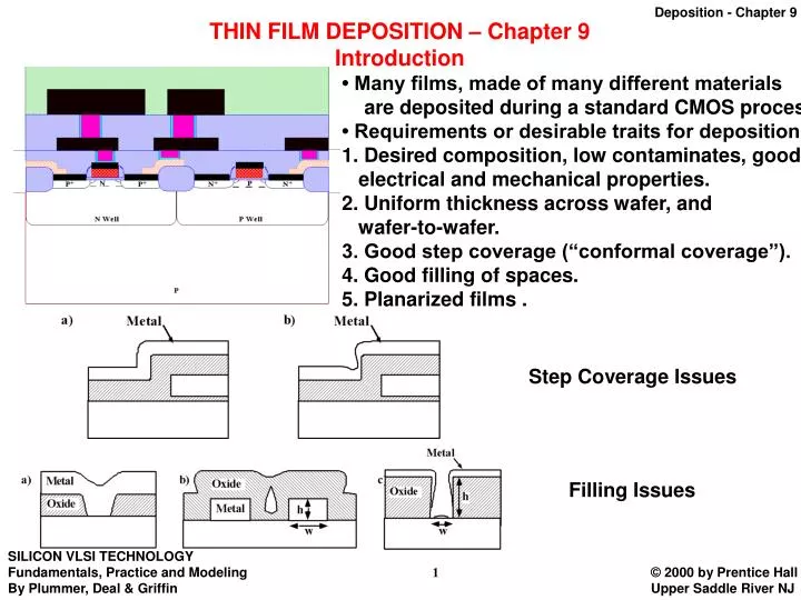
THIN FILM DEPOSITION – Chapter 9 Introduction. • Many films, made of many different materials are deposited during a standard CMOS process. • Requirements or desirable traits for deposition: 1. Desired composition, low contaminates, good electrical and mechanical properties.

E N D
THIN FILM DEPOSITION – Chapter 9 Introduction • Many films, made of many different materials are deposited during a standard CMOS process. • Requirements or desirable traits for deposition: 1. Desired composition, low contaminates, good electrical and mechanical properties. 2. Uniform thickness across wafer, and wafer-to-wafer. 3. Good step coverage (“conformal coverage”). 4. Good filling of spaces. 5. Planarized films . Step Coverage Issues Filling Issues
• Note the aspect ratios and the need for new materials. • Note also the number of metal layers requiring more deposition steps.
Historical Development and Basic Concepts Two main deposition methods are used today: 1. Chemical Vapor Deposition (CVD) 2. Physical Vapor Deposition (PVD) - APCVD, LPCVD, PECVD, HDPCVD - evaporation, sputter deposition Chemical Vapor Deposition (CVD) APCVD - Atmospheric Pressure CVD LPCVD - Low Pressure CVD
Atmospheric Pressure Chemical Vapor Deposition (APCVD) 1. Transport of reactants to the deposition region. *2. Transport of reactants from the main gas stream through the boundary layer to the wafer surface. *3. Adsorption of reactants on the wafer surface. *4. Surface reactions, including: chemical decomposition or reaction, surface migration to attachment sites (kinks and ledges); site incorporation; and other surface reactions (emission and redeposition for example). *5. Desorption of byproducts. 6. Transport of byproducts through boundary layer. 7. Transport of byproducts away from the deposition region.
F1 = diffusion flux of reactant species to the wafer = mass transfer flux, step 2 (4) where hG is the mass transfer coefficient (in cm/sec). F2 = flux of reactant consumed by the surface reaction = surface reaction flux, steps 3-5 (5) where kS is the surface reaction rate (in cm/sec). (6) In steady state: F = F1 = F2 (7) Equating Equations (4) and (5) leads to (8) The growth rate of the film is now given by where N is the number of atoms per unit volume in the film (5 x 1022 cm-3 for the case of epitaxial Si deposition) and Y is the mole fraction (partial pressure/total pressure) of the incorporating species.
1. If kS << hG, then we have the surface reaction controlled case: (9) 2. If hG << kS, then we have the mass transfer, or gas phase diffusion, controlled case: (10) • The surface term is Arrhenius with EA depending on the particular reaction (1.6 eV for single crystal silicon deposition). • hG is ≈ constant (diffusion through boundary layer). • As an example, Si epitaxial deposition is shown below (at 1 atm. total pressure). Note same EA values and hG ≈ constant. Rate is roughly proportional to (mol. wt.)-1/2.
Key points: • kS limited deposition is VERY temp sensitive. • hG limited deposition is VERY geometry (boundary layer) sensitive. • Si epi deposition often done at high T to get high quality single crystal growth. \ hG controlled. \ horizontal reactor configuration. • hG corresponds to diffusion through a boundary layer of thickness . • • But typically is not constant • as the gas flows along a surface. • special geometry is required for uniform deposition.
Low Pressure Chemical Vapor Deposition (LPCVD) • Atmospheric pressure systems have major drawbacks: • At high T, a horizontal configuration must be used (few wafers at a time). • At low T, the deposition rate goes down and throughput is again low. • The solution is to operate at low pressure. In the mass transfer limited regime, (12) But • DG will go up 760 times at 1 torr, while increases by about 7 times. Thus hG will increase by about 100 times. • Transport of reactants from gas phase to surface through boundary layer is no longer rate limiting. • Process is more T sensitive, but can use resistance heated, hot-walled system for good control of temperature and can stack wafers.
Plasma Enhanced CVD (PECVD) • Non-thermal energy to enhance processes at lower temperatures. • Plasma consists of electrons, ionized molecules, neutral molecules, neutral and ionized fragments of broken-up molecules, excited molecules and free radicals. • Free radicals are electrically neutral species that have incomplete bonding and are extremely reactive. (e.g. SiO, SiH3, F) • The net result from the fragmentation, the free radicals, and the ion bombardment is that the surface processes and deposition occur at much lower temperatures than in non-plasma systems.
High Density Plasma (HDP) CVD • Remote high density plasma with independent RF substrate bias. • Allows simultaneous deposition and sputtering for better planarization and void-free films (later). • Mostly used for SiO2 deposition in backend processes.
Physical Vapor Deposition (PVD) • PVD uses mainly physical processes to produce reactant species in the gas phase and to deposit films. • In evaporation, source material is heated in high vacuum chamber. (P < 10-5 torr). • Mostly line-of-sight deposition since pressure is low. • Deposition rate is determined by emitted flux and by geometry of the target and wafer holder.
• The evaporation source can be considered either a point source or as a small area surface source (latter is more applicable to most evaporation systems). • is the solid angle over which the source emits (4π if all directions, 2π if only upwards); N is the density of the material being deposited. • The outward flux from a point source, is independent of , while the outward flux from a small area surface source, varies as .
• Uniform thickness - use spherical wafer holder. - Point source: put source at center of sphere. - Small surface source: put source on inside surface of sphere (compensates for ). • With evaporation: • Can evaporate just about any element. • Difficult to evaporate alloys and compounds • Step coverage is poor (line of sight and Sc≈ 1). • Rarely used today. SC = 1 SC < 1
DC Sputter Deposition • Uses plasma to sputter target, dislodging atoms which then deposit on wafers to form film. • Higher pressures than evaporation - 1-100 mtorr. • Better at depositing alloys and compounds than evaporation. • The plasma contains ≈ equal numbers of positive argon ions and electrons as well as neutral argon atoms.
• Most of voltage drop of the system (due to applied DC voltage, Vc) occurs over cathode sheath. • Ar+ ions are accelerated across cathode sheath to the negatively charged cathode, striking that electrode (the “target”) and sputtering off atoms (e.g. Al). These travel through plasma and deposit on wafers sitting on anode. • Rate of sputtering depends on the sputtering yield, Y, defined as the number of atoms or molecules ejected from the target per incident ion. • Y is a function of the energy and mass of ions, and the target material. It is also a function of incident angle.
• Sputtering targets are generally large and provide a wide range of arrival angles in contrast to a point source. • Arrival angle distribution generally described by distribution (the normal component of flux striking the surface detrmines the deposition or growth rate). • Size and type of source, system geometry and collisions in gas phase important in arrival angle distribution.
RF Sputter Deposition • For DC sputtering, target electrode is conducting. • To sputter dielectric materials use RF power source. • Due to slower mobility of ions vs. electrons, the plasma biases positively with respect to both electrodes. (DC current = zero.) continuous sputtering. • When the electrode areas are not equal, the field must be higher at the smaller electrode (higher current density), to maintain overall current continuity (m = 1-2 experimentally) (13) • Thus by making the target electrode smaller, sputtering occurs "only" on the target. Wafer electrode can also be connected to chamber walls, further increasing V2/V1.
Ionized Sputter Deposition or HDP Sputtering • In some systems the depositing atoms themselves are ionized. An RF coil around the plasma induces collisions in the plasma creating the ions. • This provides a narrow distribution of arrival angles which may be useful when filling or coating the bottom of deep contact hole.
Models and Simulation • Within the past decade, a number of simulation tools have been developed for topography simulation. • Generalized picture of fluxes involved in deposition. (No gas phase boundary layer is included, so this picture doesn't fully model APCVD.) • Essentially the same picture will be used for etching simulation (in Chapter 10). (14) • To simulate these processes, we need mathematical descriptions of the various fluxes. • Modeling specific systems involves figuring out which of these fluxes needs to be included.
• Direct fluxes ( ) are generally modeled with an arrival angle distribution just above the wafer (doesn't model equipment). (15) • is the normal component of the incoming flux (which is what is needed in determining the growth rate). • Higher pressure systems more gas phase collisions, shorter mean free path n = 1 (isotropic arrival). • Lower pressure systems fewer gas phase collisions, longer mean free path n > 1 (anisotropic arrival). • Ionic species in biased systems directed arrival n > 1 (anisotropic arrival). • Once the direct fluxes are known, surface topography must be considered. • Surface orientation, viewing angle and shadowing are important. Gas phase collisions are neglected near the wafer surface.
• The indirect fluxes are associated with processes on the wafer surface. • Surface diffusion is driven by the local curvature of the surface (to minimize the surface free energy) and is given by (16) where DS is the surface diffusivity, is the surface energy, K is the curvature and are constants. • Surface diffusion helps to fill in holes, and produces more planar depositions because molecules can diffuse to "smooth out" the topography. • arises because not all molecules "stick" when they arrive at the surface. (17) where SC is the sticking coefficient. High (Sc = 1) Low (Sc < 1) (18) • Generally ions are assumed to stick (SC = 1), neutrals have SC < 1 and are assumed to be emitted with a angle distribution (no memory of arrival angle).
• arises because the emitted flux can land elsewhere on the surface. Thus (19) • The redeposited flux at point i due to an emitted flux at point k can then be summed over all i and k. accounts for the geometry between i and k. • Thus a low SC < 1 can produce more conformal coverage because of emission/redeposition (usually more important than surface diffusion in CVD). • The sputtered flux is caused primarily by energetic incoming ions. where Y is the sputtering yield. • Y is angle sensitive which can be used to achieve more planar surfaces during deposition (example later). (20) • The sputtered molecules can be redeposited. This is modeled as in Eqn. (19), i.e. (21)
• Finally, ions striking the surface can sometime enhance the deposition rate (by supplying the energy to drive chemical reactions for example), so that (22) LPCVD Deposition Systems • In these systems there are no ions involved and hence no sputtering. Surface diffusion also is usually not important.
• The sticking coefficient SC is small in these systems so there will be significant desorbed (emitted) and redeposited fluxes. • Thus at each point on the surface, (23) • We define the deposition flux at each point, so the deposition rate is simply given as: (24) where N is the film density. • distribution is used for the incoming molecules.
PECVD Deposition Systems • In these systems an ion flux can enhance the deposition rate by changing the surface reactions. Sputtering is usually not significant because the ion energy is low, nor is direct deposition of ions significant. (25) • Thus where Kd and KI are relative rate constants for the neutral and ion-enhanced components respectively.
PVD Deposition Systems • Standard PVD systems might include DC and RF sputtering systems and evaporation systems. • Ions generally do not play a significant role in these systems, so modeling is similar to LPCVD systems. Thus (26) • The values for Sc and would be different for LPCVD and PVD systems however. • Sometimes these systems are operated at high temperatures, so a surface diffusion term must be added. (27)
Ionized PVD Deposition Systems • These systems are complex to model because both ions and neutrals play a role. • They are often used for metal deposition so that Ar+ ions in addition to Al+ or Ti+ ions may be present. • Thus almost all the possible terms are included where Fd includes the direct and redeposited (emitted) neutral fluxes, Fi includes the direct and ion-induced fluxes associated with the ions, and Frd models redeposition due to sputtering.
High Density Plasma CVD Deposition Systems • Very similar to IPVD (except neutral direct flux not as important): (29)
Models in SPEEDIE LPCVD: PECVD: Standard PVD: High T PVD: Ionized PVD: HDP CVD:
J.P. McVittie, J.C. Rey, L.Y. Cheng, and K.C. Saraswat, "LPCVD Profile Simulation Using a Re-Emmission Model", IEDM Tech. Digest, 917-919 (1990). L-Y. Cheng, J. P. McVittie and K. C. Saraswat, " Role of Sticking Coefficient on the Deposition Profiles of CVD Oxide, "Appl. Phys. Lett., 58(19), 2147-2149 (1991).
PECVD LPCVD J.P. McVittie, “Test Structure and Modeling Studies of Deposition and Etch Mechanisms”, Talk TC1-WeM6, AVS mtg in Orlando, Florida, 1993
Parameter Values for Specific Systems • • PVD systems - more vertical arrival angle distribution (low pressure line of sight • or field driven ions). n > 1 typically. • • CVD systems provide isotropic arrival angle distributions (higher pressure, • gas phase collisions, mostly neutral molecules). n ≈ 1 typically. • • PVD systems usually provide Sc of 1. Little surface chemistry involved. Atoms • arrive and stick. • • CVD systems involve surface chemistry and Sc <<1. Molecules often reemit and • redeposit elsewhere before reacting. • CVD systems provide more conformal deposition.
Topography Simulation (Using SPEEDIE) • SPEEDIE simulations for LPCVD deposition of SiO2 with Sc = 1 (which is more typical of PVD than LPCVD) and varying values of n, the arrival angle distribution factor: (a) n=1; (c) n=10. • Worse step coverage results as n increases (the arrival angle distribution narrows). • Even for n = 1, conformal coverage is not achieved. • SPEEDIE simulations for LPCVD deposition of SiO2 in a narrow trench with the same isotropic arrival angle distribution (n=1) but different values of Sc: (a) Sc = 1; (b) Sc = 0.1; and (c) Sc = 0.01. • Reducing Sc is much more effective than changing n if conformal deposition is desired.
• Results of SPEEDIE LPCVD simulations with the sidewall angle changed. Sc = 0.2 and n = 1. Note the improved trench filling. 90˚ 85˚ 80˚ • SPEEDIE simulations comparing LPCVD and HDPCVD depositions. (a) LPCVD deposition of SiO2 over rectangular line. Sc = 0.1 and n = 1. (b) HDPCVD deposition, with directed ionic flux and angle-dependent sputtering, over rectangular line showing much more planar topography. • CMP might still be required in the HDPCVD case to fully planarize the surface.
• SPEEDIE simulations comparing LPCVD and HDPCVD depositions. (c) LPCVD deposition in trench, showing void formation. Sc = 0.2 and n = 1. (d) HDPCVD deposition in trench, showing much better filling. • HDPCVD has a strong directed ion component and any overhangs that form are sputtered away. • Actual SEM images of HDP oxide deposition.
Summary of Key Ideas • Thin film deposition is a key technology in modern IC fabrication. • Topography coverage issues and filling issues are very important, especially as geometries continue to decrease. • CVD and PVD are the two principal deposition techniques. • CVD systems generally operate at elevated temperatures and depend on chemical reactions. • In general either mass transport of reactants to the surface or surface reactions can limit the deposition rate in CVD systems. • In low pressure CVD systems, mass transport is usually not rate limiting. • However even in low pressure systems, shadowing by surface topography can be important. • In PVD systems arrival angle distribution is very important in determining surface coverage. Shadowing can be very important. • A wide variety of systems are used in manufacturing for depositing specific thin films. • Advanced simulation tools are becoming available, which are very useful in predicting topographic issues. • Generally these simulators are based on physical models of mass transport and surface reactions and utilize parameters like arrival angle and sticking coefficients from direct and indirect fluxes to model local deposition rates.