Download
1 / 9
90 likes | 184 Views
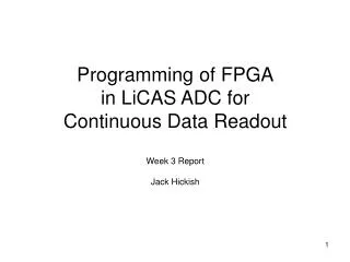
Programming of FPGA in LiCAS ADC for Continuous Data Readout Jack Hickish. Programming the FPGA. Current Situation – FSI Modifications made Still to do…. Sampling / Manipulation of data. External FIFO. FFI Operation. RAM. FIFO. Data Out over USB. The Current Situation - FSI. Data In.

E N D
Programming of FPGAin LiCAS ADC forContinuous Data Readout Jack Hickish
Programming the FPGA • Current Situation – FSI • Modifications made • Still to do…
Sampling / Manipulation of data External FIFO FFI Operation RAM FIFO Data Out over USB The Current Situation - FSI Data In
FFI Operation Data In Choice of FFI Data Path - Preserves ‘Test Mode’ feature and existing sampling method and rate controls - Requires no components outside the FPGN, for ease of simulation - USB interface requires some sort of memory buffer to compensate for fluctuations in USB data transfer rate Sampling / Manipulation FIFO Data Out over USB
Data Path Data needs to be rerouted bypassing external RAM and FIFO Sampling Data is only taken for a fixed number of clock cycles. Data is only output after sampling period is complete. Read/write enabling system incompatible with constant readout Internal Control Signals Obstacles to FFI Operation
Modifications New registry entries added to control operation mode New entries: “FFI MODE” bit 1 for FFI operation 0 for FSI operation Data Bus and Control signals (including sampling controls) intercepted by new components, which redirect and alter signals based on the state of the FFI MODE bit. “STOP” bit halts FFI operation Data Path Sampling Internal Control Signals
Sampling / Manipulation of data External FIFO Data In FFI Operation RAM FIFO Data Out over USB Modifications
bit = 1 Data in direct from Sampling control FIFO bit = 0 Data in from RAM USB Output “data_path_selector” FFI mode bit Modifications
Still to do… • Simulation • Output Data Rate • Clock Divider • Extension of existing sampling rate settings • Diagnostics • Notification (LED?) in case of failure in data path