Download
1 / 86
860 likes | 1.05k Views
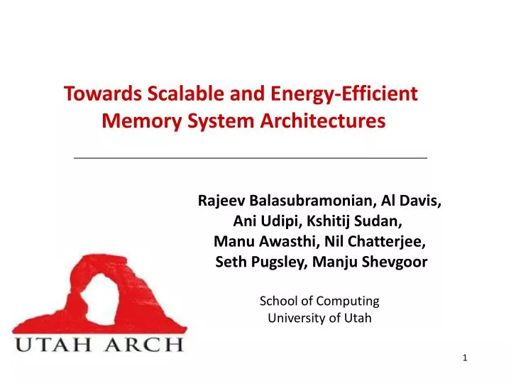
Towards Scalable and Energy-Efficient Memory System Architectures. Rajeev Balasubramonian , Al Davis, Ani Udipi , Kshitij Sudan, Manu Awasthi , Nil Chatterjee , Seth Pugsley , Manju Shevgoor School of Computing University of Utah. Towards Scalable and Energy-Efficient

E N D
Towards Scalable and Energy-Efficient Memory System Architectures Rajeev Balasubramonian, Al Davis, AniUdipi, Kshitij Sudan, Manu Awasthi, Nil Chatterjee, Seth Pugsley, ManjuShevgoor School of Computing University of Utah
Towards Scalable and Energy-Efficient Memory System Architectures
Convergence of Technology Trends Energy New Memory Technologies Overhaul of main memory architecture! BW, Capacity, and Locality for Multi-Cores Reliability
High Level Approach • Explore changes to memory chip microarchitecture • Must cause minimal disruption to density • Explore changes to interfaces and standards • Major change appears inevitable! • Explore system and memory controller innovations • Most attractive, but order-of-magnitude improvement unlikely • Design solutions that are technology-agnostic
Projects • Memory Chip • Reduce overfetch • Support reliability • Handle PCM drift • Promote read/write • parallelism • Memory Interface • Interface with • photonics • Organize channel • for high capacity • Memory Controller • Maximize use of • row buffer • Schedule for low • latency and energy • Exploit mini-ranks DIMM CPU … MC
Talk Outline • Mature work: • SSA architecture – Single Subarray Access (ISCA’10) • Support for reliability (ISCA’10) • Interface with photonics (ISCA’11) • Micro-pages – data placement for row buffer efficiency (ASPLOS’10) • Handling multiple memory controllers (PACT’10) • Managing resistance drift in PCM cells (NVMW’11) • Preliminary work: • Handling read/write parallelism • Enabling high capacity • Handling DMA scheduling • Exploiting rank subsetting for performance and thermals
Minimizing Overfetch with Single Subarray Access AniUdipi Primary Impact DIMM CPU … MC
Problem 1 - DRAM Chip Energy • On every DRAM access, multiple arrays in multiple chips are activated • Was useful when there was good locality in access streams • Open page policy • Helped keep density high and reduce cost-per-bit • With multi-thread, multi-core and multi-socket systems, there is much more randomness • “Mixing” of access streams when finally seen by the memory controller
Rethinking DRAM Organization • Limited use for designs based on locality • As much as 8kbytes read in order to service a 64byte cache line request • Termed “overfetch” • Substantially increases energy consumption • Need a new architecture that • Eliminates overfetch • Increases parallelism • Increases opportunity for power-down • Allows efficient reliability
Proposed Solution – SSA Architecture ONE DRAM CHIP ADDR/CMD BUS DIMM 64 Bytes Subarray Bitlines Bank Row buffer 8 8 8 8 8 8 8 8 8 DATA BUS MEMORY CONTROLLER Global Interconnect to I/O
SSA Basics • Entire DRAM chip divided into small “subarrays” • Width of each subarray is exactly one cache line • Fetchentirecache line from a single subarray in a single DRAM chip – SSA • Groups of subarrays combined into “banks” to keep peripheral circuit overheads low • Close page policy and “posted-RAS” • Data bus to processor essentially split into 8 narrow buses
SSA Architecture Impact • Energy reduction • Dynamic – fewer bitlines activated • Static – smaller activation footprint – more and longer spells of inactivity – better power down • Latency impact • Limited pins per cache line – serialization latency • Higher bank-level parallelism – shorter queuing delays • Area increase • More peripheral circuitry and I/O at finer granularities – area overhead (< 5%)
Area Impact • Smaller arrays – more peripheral overhead • More wiring overhead in the on-chip interconnect between arrays and pin pads • We did a best-effort area impact calculation using a modified version of CACTI 6.5 • Analytical model, has its limitations • More feedback in this specific regard would be awesome! • More info on exactly where in the hierarchy overfetch stops would be great too
Support for Chipkill Reliability AniUdipi Primary Impact DIMM CPU … MC
Problem 2 – DRAM Reliability • Many server applications require chipkill-level reliability – failure of an entire DRAM chip • One example of existing systems • Consider baseline 64-bit word plus 8-bit ECC • Each of these 72 bits must be read out of a different chip, else a chip failure will lead to a multi-bit error in the 72-bit field – unrecoverable! • Reading 72 chips - significant overfetch! • Chipkill even more of a concern for SSA since entire cache line comes from a single chip
Proposed Solution DIMM DRAM DEVICE Approach similar to RAID-5 L0 C L1 C L2 C L3 C L4 C L5 C L6 C L7 C P0 C L9 C L10 C L11 C L12 C L13 C L14 C L15 C P1 C L8 C .. .. .. .. .. .. .. .. .. P7 C L56 C L57 C L58 C L59 C L60 C L61 C L62 C L63 C L – Cache Line C – Local Checksum P – Global Parity
Chipkill design • Two-tier error protection • Tier - 1 protection – self-contained error detection • 8-bit checksum/cache line – 1.625% storage overhead • Every cache line read is now slightly longer • Tier -2 protection – global error correction • RAID-like striped parity across 8+1 chips • 12.5% storage overhead • Error-free access (common case) • 1 chip reads • 2 chip writes – leads to some bank contention • 12% IPC degradation • Erroneous access • 9 chip operation
Questions • What are the common failure modes in DRAM? PCM? • Do entire chips fail? • Do parts of chips fail? • Which parts? Bitlines? Wordlines? Capacitors? • Entire arrays? • Entire banks? • I/O? • Should all these failures be handled the same way?
Designing Photonic Interfaces AniUdipi Primary Impact DIMM CPU … MC
Problem 3 – Memory interconnect • Electrical interconnects are not scaling well • Where can photonics make an impact, both on energy and performance? • Various levels in the DRAM interconnect • Memory cell to sense-amp - addressed by SSA • Row buffer to I/O – currently electrical (on-chip) • I/O pins to processor – currently electrical (off-chip) • Photonic interconnects • Large static power component – laser/ring tuning • Much lower dynamic component – relatively unaffected by distance • Electrical interconnects • Relatively small static component • Large dynamic component • Cannot overprovision photonic bandwidth, use only where necessary
Consideration 1 – How much photonics on a die? Photonic Energy Electrical Energy
Consideration 2 - Increasing Capacity • 3D stacking is imminent • There will definitely be several dies on the channel • Each die has photonic components that are constantly burning static power • Need to minimize this! • TSVs available within a stack; best of both worlds • Large bandwidth • Low static energy • Need to exploit this!
Proposed Design DRAM chips Memory controller Processor DIMM Photonic Interface die + Stack controller Waveguide
Proposed Design – Interface Die • Exploit 3D die stacking to move all photonic components to a separate interface die, shared by several memory dies • Use photonics where there is heavy utilization – shared bus between processor and interface die i.e. the off-chip interconnect • Helps break pin barrier for efficient I/O, substantially improves socket-edge BW • On-stack, where there is low utilization, use efficient low-swing interconnects and TSVs
Advantages of the proposed system • Reduction in energy consumption • Fewer photonic resources, without loss in performance • Rings, couplers, trimming • Industry considerations • Does not affect design of commodity memory dies • Same memory die can be used with both photonic and electrical systems • Same interface die can be used with different kinds of memory dies – DRAM, PCM, STT-RAM, Memristors
Problem 4 – Communication Protocol • Large capacity, high bandwidth, and evolving technology trends will increase pressure on the memory interface • Need to handle heterogeneous memory modules, each with its own maintenance requirements, further complicates scheduling • Very little interoperability – affects both consumers (too many choices!) and vendors (stock-keeping and manufacturing) • Heavy pressure on address/command bus – several commands to micro-manage every operation of the DRAM • Several independent banks – need to maintain large amounts of state to schedule requests efficiently • Simultaneous arbitration for multiple resources (address bus, data bank, data bus) to complete a single transaction
Proposed Solution – Packet-based interface • Release most of the tight control memory controller holds today • Move mundane tasks to the memory modules themselves (on the interface die) - make them more autonomous • maintenance operation (refresh, scrub, etc.) • routine operations (DRAM precharge, NVM wear handling) • timing control (DRAM alone has almost 20 different timing constraints to be respected) • coding and any other special requirements • Only information the memory module needs is the address and read/write identification, time slots reserved apriori for data return
Advantages • Better interoperability, plug and play • As long as the interface die has the necessary information, everything in interchangeable • Better support for heterogeneous systems • Allows easier data movement between DRAM and NVM for example, on the same channel • Reduces memory controller complexity • Allows innovation and value addition in the memory, without being constrained by processor-side support • Reduces bit transport energy on the address/command bus
Data Placement with Micro-Pages To Boost Row Buffer Utility Kshitij Sudan Primary Impact DIMM CPU … MC
DRAM Access Inefficiencies • Over fetch due to large row-buffers • 8 KB read into row buffer for a 64 byte cache line • Row-buffer utilization for a single request < 1% • Diminishing locality in multi-cores • Increasingly randomized memory access stream • Row-buffer hit rates bound to go down • Open page policy and FR-FCFS request scheduling • Memory controller schedules requests to open row-buffers first • Goal • Improve row-buffer hit-rates for Chip Multi-Processors
Key Observation Cache Block Access Pattern Within OS Pages • Gather all heavily accessed chunks of independent OS pages and map them to the same DRAM row For heavily accessed pages in a given time interval, accesses are usually to a few cache blocks
Basic Idea Reserved DRAM Region 4 KB OS Pages 1 KB micro-pages DRAM Memory Coldest micro-pages Hottest micro-pages
Hardware Implementation (HAM) Hardware Assisted Migration (HAM) Baseline 4 GB Main Memory CPU Memory Request Physical Address X Page A X Mapping Table Old Address New Address X Y 4 MB Reserved DRAM region Y New addr . Y
Results • 5M cycle EPOCH, ROPS, HAM and ORACLE Percent change in performance Apart from average 9% performance gains, our schemes also save DRAM energy at the same time!
Conclusions • On average, for applications with room for improvement and with our best performing scheme • Average performance ↑9% (max. 18%) • Average memory energy consumption ↓18%(max. 62%). • Average row-buffer utilization ↑ 38% • Hardware assisted migration offers better returns due to fewer overheads of TLB shoot-down and misses
Data Placement Across Multiple Memory Controllers Kshitij Sudan Primary Impact DIMM CPU … MC
DRAM NUMA Latency DIMM DIMM DIMM DIMM DIMM DIMM MC MC Core 1 Core 2 Core 1 Core 2 Core 3 Core 4 Core 3 Core 4 On-Chip Memory Controller MC QPI QPI Interconnect DIMM DIMM DIMM DIMM DIMM DIMM Memory Channel MC MC Core 1 Core 2 Core 1 Core 2 DIMM DRAM (DIMMs) Core 3 Core 4 Core 3 Core 4 Socket Boundary
Problem Summary • Pin limitations → increasing queuing delay • Almost 8x increase in queuing delays from single core/one thread to 16 cores/16 threads • Multi-cores → increasing row-buffer interference • Increasingly randomized memory access stream • Longer on- and off-chip wire delays → increasing NUMA factor • NUMA factor already at 1.5x today • Goal • Improve application performance by reducing queuing delays and NUMA latency
Policies to Manage Data Placement Among MCs • Adaptive First Touch • Assign new virtual pages to a DRAM (physical) page belonging to MC(j) minimizing the a cost function • Dynamic Page Migration • Programs change phases →Imbalance in MC load • Migrate pages between MCs at runtime • Integrating Heterogenous Memory Technologies cost j = α x loadj + β x rowhitsj + λ x distancej costk = Λ * distancek + Γ * rowhitsk cost j = α x loadj + β x rowhitsj + λ x distance + Ƭ x LatencyDimmClusterj+ µ x Usagej
Summary • Multiple on-chip MCs will be common in future CMPs • Multiple cores sharing one MC, MCs controlling different types of memories • Intelligent data mapping needed • Adaptive First Touch policy (AFT) • Increases performance by 6.5% in homogeneous and by 1.6% in DRAM – PCM hierarchy. • Dynamic page migration, improvement on AFT • Further improvement over AFT - 8.9% over baseline in homogeneous, and by 4.4% in best performing DRAM-PCM hierarchy.
Managing Resistance Drift in PCM Cells Manu Awasthi Primary Impact DIMM CPU … MC
Quick Summary • Multi level cells in PCM appear imminent • A number of proposals exist to handle hard errors and lifetime issues of PCM devices • Resistance Drift is a less explored phenomenon • Will become increasingly significant as number of levels/cell increases – primary cause of “soft errors” • Naïve techniques based on DRAM-like refresh will be extremely costly for both latency and energy • Need to explore holistic solutions to counter drift
What is Resistance Drift? Time 11 10 01 00 ERROR!! Tn B T0 A Resistance Crystalline Amorphous
Resistance Drift Data (11) (01) (10) (00)
Resistance Drift - Issues • Programmed resistance drifts according to power law equation - • R0, α usually follow a Gaussian distribution • Time to drift (error) depends on • Programmed resistance (R0), and • Drift Coefficient (α) • Is highly unpredictable!! Rdrift(t) = R0х (t)α
Resistance Drift - How it happens ERROR!! 11 10 01 00 Number of Cells R0 R0 Rt Rt • Median case cell • Typical R0 • Typical α • Worst case cell • High R0 • High α Scrub rate will be dictated by the Worst Case R0 and Worst Case α Naive refresh/scrub will be extremely costly!
Architectural Solutions - Headroom • Assumes support for Light Array Reads for Drift Detection (LARDDs) & ECC-N • Headroom-h scheme – scrub is triggered if N-h errors are detected • Decreases probabilityof errors slipping through • Increases frequency of full scrub and hence decreases life time • Gradual Headroom scheme : Start with large LARDD frequency, increase frequency as errors increase Read Line Check for Errors True Errors < N-h After N cycles False Scrub Line
Reducing Overheads with Circuit Level Solution • Invoking ECC on every LARDD increases energy consumption • Parity – like error detection circuit is used to signal the need for a full fledged ECC error detect • Number of Drift Prone States in each line are counted when the line is written into memory (single bit represents odd/even) • At every LARDD, parity is verified • Reduces need for ECC read-compare at every LARDD cycle (11) (01) (10) (00) 48
More Solutions • Precise Writes • More write iterations to program state closer to mean, reduce chance of drift • Increases energy consumption , write time and decreases lifetime! • Non Uniform Guardbanding • Resistance is equally distributed between all n states • Expand resistance range for drift prone states at expense of non-drift prone ones
Results Errors LARDD Interval (seconds)