Download
1 / 1
10 likes | 92 Views
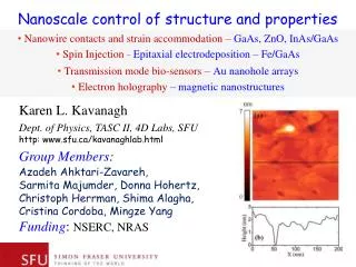
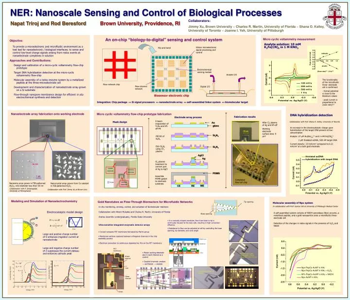
0.5. 0.0. 2.0. r 0. 1.5. -0.5. cathodic. 1.0. 0.5. Current (nA). Peak current (nA). -1.0. 0.0. 0.2. 0.4. 0.6. 0.8. 1.0. -0.5. Npx-PepCo-AuNP in KAc. -1.0. -1.5. anodic. -1.5. Npx-PepCo-AuNP in KAc + H 2 O 2. -2.0. NPx-PepCo-AuNP in KAc + NADH. -2.0. (Scan rate) 1/2.

E N D
0.5 0.0 2.0 r0 1.5 -0.5 cathodic 1.0 0.5 Current (nA) Peak current (nA) -1.0 0.0 0.2 0.4 0.6 0.8 1.0 -0.5 Npx-PepCo-AuNP in KAc -1.0 -1.5 anodic -1.5 Npx-PepCo-AuNP in KAc + H2O2 -2.0 NPx-PepCo-AuNP in KAc + NADH -2.0 (Scan rate)1/2 (V/s)1/2 Npx-AuNP in KAc -2.5 0.8 0.6 0.4 0.2 0.0 -0.2 Silicon microelectronic signal processing and control Flip and bond Potential vs. Ag/AgCl (V) Electrochemical sensing module Flow network chip Flow-channel network Biosensor electronic chip E-beam evaporation of Ti/Au and lift-off PR 30 µm PECVD of Si3N4 Etch Si3N4 using CF4 plasma Cl2 plasma treatment to convert part of Ag to AgCl Assemble PDMS gasket to electrode substrate Tip opening Base opening PET membrane PDMS channel 14 12 T = 107 12 Inlet 10 ZZ = 0 ZZ = −3 10 8 8 ZO = +3 +2 +1 0 −1 −2 −3 6 Glass channel Current density, FDC/r Current density, FDC/r 6 4 4 2 2 0 0 -20 -15 -10 -5 -20 -15 -10 -5 0 5 10 15 20 0 5 10 15 20 Voltage, RT/F Voltage, RT/F Outlet NER: Nanoscale Sensing and Control of Biological Processes Collaborators: Jimmy Xu, Brown University ~Charles R. Martin, University of Florida ~ Shana O. Kelley, University of Toronto ~ Joanne I. Yeh, University of Pittsburgh Napat Triroj and Rod Beresford Brown University, Providence, RI Micro cyclic voltammetry measurement An on-chip “biology-to-digital" sensing and control system • Objective: • To provide a microelectronic and microfluidic environment as a test bed for nanoelectronic / biological interfaces; to sense and control low-level charge signals arising from redox events at nanoelectrode complexes in solution • Approaches and Contributions: • Design and calibration of a micro-cyclic voltammetry flow-chip prototype • Target DNA hybridization detection at the micro-cyclic voltammetry flow-chip • Molecular assembly of a redox enzyme system by a metallized peptide at the three-microelectrode cell • Development and characterization of nanoelectrode array grown on a Si substrate • Flow-through nanopore membrance design for efficient in situ electrochemical synthesis and detection Analyte solution: 10 mM K3Fe(CN)6 in 1 M KNO3 Analyte I/O • The functionality of the microfluidic three- electrode cell is confirmed: • formal potential is close to the literature values • peak current is proportional to (scan rate)1/2 Digital I/O Integration: Chip package Si signal processors nanoelectrode array self-assembled linker system biomolecular target Nanoelectrode array fabrication onto working electrode Micro cyclic voltammetry flow-chip prototype fabrication DNA hybridization detection Fabrication results Electrode array process Mask design Collaboration with Prof. Shana O. Kelley, University of Toronto After Cl2 plasma of Ag and lift-off Working electrode surface area: 9 µm2 An increase in the electrocatalytic charge upon hybridization of the target DNA present at low-concentration Analyte: 27 µM Ru(NH3)63+ and 2 mM Fe(CN)63- 2 µM thiolated ssDNA, 500 nM target DNA Current density: 3.9 mA/cm2 compared to 0.21 mA/cm2 at a bulk gold electrode Au dot 1 μm Completed flow-cell chip Nanowire array grown in FIB-patterned Al2O3; wire diameter less than 50 nm Nanocrystal array grown from Co catalyst in FIB-patterned Al2O3 Collaboration with P. Jaroenapibal, University of Pennsylvania Collaboration with Prof. Jimmy Xu at Brown Univ. Modeling and Simulation of Nanoelectrochemistry Gold Nanotubes as Flow-Through Bioreactors for Microfluidic Networks Molecular assembly of Npx system In collaboration with Prof. Joanne Yeh at University of Pittsburgh Medical Center In situ monitoring, sensing, control, and actuation of biomolecular reactions Collaboration with Hitomi Mukaibo and Charles R. Martin, University of Florida Andres Jaramillo (undergraduate), Florida State University Electrocatalytic model design A self-assembled system consists of NADH peroxidase (Npx) enzyme, a metallized peptide, and a gold nanoparticle onto a microfluidic three-electrode cell Detection of the changes in redox signals in the presence of H2O2 and NADH • In a conically shaped nanotube, flow from base to tip is continually focused to the tube wall, resulting in high conversion efficiency • Resistance to flow can be adjusted at will by controlling the base opening, tip diameter, and cone angle Voltage T Ultra-sensitive integrated enzymatic detector arrays membrane contact pad Time • Conical nanopore PET membrane fabricated by Martin group • Membrane sections captured between orthogonal channels in the chip assembly process • Electrical connection to continuous deposited Au film on the PET membrane Large and positive charge number of O enhances migration current at nanoelectrode Large and negative charge number of Z suppresses the current plateau and enhances cathodic peak • Planar working electrode also in each channel as a control • Coupled channels: analyze → synthesize →analyze Electrode cell in glass: channel depth = 12 μm area of WE = 2.5 x 10⁻⁵ cm2 Continuity of Au trace into channel