Download
1 / 1
10 likes | 105 Views
Introduction. A Verilog-A compact model for Surrounding Gate Transistors (SGTs) has been implemented to study both basic analog and digital circuits. The main features of CMOS inverters based on the novel SGTs have been analyzed.

E N D
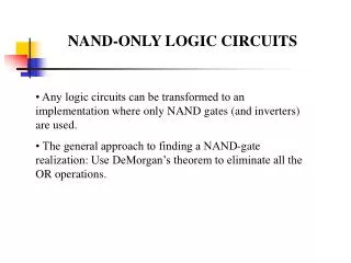
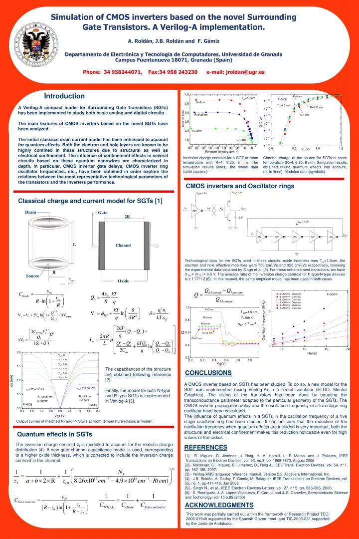
Introduction A Verilog-A compact model for Surrounding Gate Transistors (SGTs) has been implemented to study both basic analog and digital circuits. The main features of CMOS inverters based on the novel SGTs have been analyzed. The initial classical drain current model has been enhanced to account for quantum effects. Both the electron and hole layers are known to be highly confined in these structures due to structural as well as electrical confinement. The influence of confinement effects in several circuits based on these quantum nanowires are characterized in depth. In particular, CMOS inverter gate delays, CMOS inverter ring oscillator frequencies, etc., have been obtained in order explore the relations between the most representative technological parameters of the transistors and the inverters performance. Inversion charge centroid for a SGT at room temperature with R=4, 6.25, 8 nm. The simulation results (lines), the model data (solid squares) Channel charge at the source for SGTs at room temperature (R=4, 6.25, 8 nm). Simulation results, obtained taking quantum effects into account, (solid lines), Modeled data (symbols). CMOS inverters and Oscillator rings VDD= 1.2V VDD= 1.2V Classical charge and current model for SGTs [1] VIN in out VOUT Drain Gate INV 2R 5 fF VDD= 1.2V in VOUT INV INV INV INV INV L Channel Technological data for the SGTs used in these circuits: oxide thickness was Tox=1.5nm, the electron and hole effective mobilities were 750 cm2/Vs and 325 cm2/Vs respectively, following the experimental data obtained by Singh et al. [5]. For these enhancement transistors, we have VTN ≈ |VTP| ≈ 0.5 V. The average ratio of the inversion charge centroid for P-type/N-type devices is z 1.77/1.2 [6]; in this respect, the same empirical model has been used in both cases. R Source tox Oxide Simulation of CMOS inverters based on the novel Surrounding Gate Transistors. A Verilog-A implementation. A. Roldán, J.B. Roldán and F. Gámiz Departamento de Electrónica y Tecnología de Computadores, Universidad de GranadaCampus Fuentenueva 18071, Granada (Spain) Phone: 34 958244071, Fax:34 958 243230 e-mail: jroldan@ugr.es The capacitances of the structure are obtained following reference [2]. Finally, the model for both N-type and P-type SGTs is implemented in Verilog-A [3]. CONCLUSIONS A CMOS inverter based on SGTs has been studied. To do so, a new model for the SGT was implemented (using Verilog-A) in a circuit simulator (ELDO, Mentor Graphics). The sizing of the transistors has been done by equating the transconductance parameter adapted to the particular geometry of the SGTs. The CMOS inverter propagation delay and the oscillation frequency of a five stage ring oscillator have been calculated. The influence of quantum effects in a SGTs in the oscillation frequency of a five stage oscillator ring has been studied. It can be seen that the reduction of the oscillation frequency when quantum effects are included is very important, both the structural and electrical confinement makes this reduction noticeable even for high values of the radius. Output curves of matched N- and P- SGTs at room temperature (classical model). Quantum effects in SGTs The inversion charge centroid zI is modelled to account for the realistic charge distribution [4]. A new gate-channel capacitance model is used, corresponding to a higher oxide thickness, which is corrected to include the inversion charge centroid in the channel. REFERENCES [1].-B. Iñiguez, D. Jiménez, J. Roig, H. A. Hamid, L. F. Marsal and J. Pallares, IEEE Transactions on Electron Devices, vol. 52, no.8, pp. 1868-1873, August 2005 [2].- Moldovan, O., Iniguez, B., Jimenez, D., Roig J., IEEE Trans. Electron Devices, vol. 54, nº 1, pp. 162-165, 2007. [3].- Verilog-AMS language reference manual, Version 2.2, Accellera International, Inc. [4].- J.B. Roldán, A. Godoy, F. Gámiz, M. Balaguer, IEEE Transactions on Electron Devices, vol. 55, no. 1, pp 411-416, Jan 2008. [5].- Singh N., et al., IEEE Electron Devices Letters, vol. 27, nº 5, pp. 383-386, 2006. [6].- S. Rodríguez, J. A. López-Villanueva, P. Cartujo and J. E. Carceller, Semiconductor Science and Techonolgy, vol. 15 p.85 (2000) ACKNOWLEDGMENTS This work was partially carried out within the framework of Research Project TEC-2005-01948 supported by the Spanish Government, and TIC-2005-831 supported by the Junta de Andalucía.