Download
1 / 42
500 likes | 835 Views
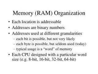
Chapter6. Memory Organization. Transfer between P and M should be such that P can operate at its maximum speed. → not feasible to use a single memory using one technology. – CPU registers : a small set of high-speed registers in P as working memory for

E N D
Transfer between P and M should be such that P can operate at its maximum speed. → not feasible to use a single memory using one technology. – CPU registers : a small set of high-speed registers in P as working memory for temporary storage of instructions and data. Single clock cycle access. – Main(primary) memory : can be accessed directly and rapidly by CPU. While an IC technology is similar to that of CPU registers, access is slower because of large capacity and physical separation from CPU – Secondary(back up) memory : much larger in capacity, much slower, and much cheaper than main memory. – Cache : an intermediate temporary storage unit between processor registers and main-memory. One to three clock cycle access.
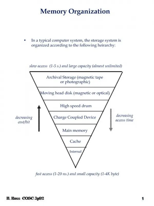
The objective of memory design is to provide adequate storage capacity with an acceptable level of performance and cost. ⇒ memory hierarchy, automatic storage concepts, virtual memory concepts, and the design of communication link. Memory Device Characteristics 1. Cost C = P/S (dollars/bits) 2. Access time(tA) : the average time required to read one word from the memory. From the time a read request is received by memory to the time when all the requested information has been made at the memory output. depending on the physical nature of the storage medium and on the access mechanism used. Memory units with fast access are expensive. 3. Access mode RAM(Random Access Memory) : accessed in any order and access time is independent of the location. Serial-access memory(tape)
4. Alterability : ROM(Read Only Memory), PROM(Programmable…), EPROM(Extended…). 5. Performance of storage : destructive readout, dynamic storage, and volatility. ex) dynamic memory(DRAM) – required periodic refreshing. static random access memory(SRAM) – require no periodic refreshing. DRAM is much cheaper then SRAM “volatile” : if the stored information can be destroyed by a power failure. 6. Cycle time(tM) : the mean time that must elapse between the initiation of two consecutive access operations. tM can be greater than tA. ( Dynamic memory can’t initiate a new access until a refresh operation) 7. Physical characteristics – Storage density – Reliability : MTBF.
RAM : The access and cycle times for every location are constant and independent of its position.
Array organization : The memory address is partitioned into d components so that the address Ai of cell ci becomes a d-dimensional vector (Ai1, Ai2, ··· ,Aid)=Ai. Each of d parts goes to a different decoder → d-dimensional array. Usually, we use 2-dimensional array organization. If less access circuitry and less time. 2-D memory organization matches well the circuit structure by IC technology. Key issue: How to reduce access time, fault-tolerant techniques 6.2 Memory Systems : A hierarchical storage system managed by operating system. 1. To free programmers from the need to carry out storage allocation and to permit efficient sharing of memory space among different users. 2. To make programs independent of the configuration and the capacity of the memory systems used during their execution. 3. To achieve the high access rates and low cost per bit that is possible with a memory hierarchy implemented by an automatic address mapping mechanism. A typical hierarchy of memory ( M1, M2, ··· , Mk ).
Generally, all information in Mi-1 at any time is also stored in Mi, but not vice versa. Let, Ci: cost per bit – Ci > C i+1 tAi: access time – tAi < tAi+1 Si: storage space Si < Si+1
If the address which CPU generates is currently assigned only to Mi for i 1, the execution of the program must be suspended until reassigned from Mi to M1. → very slow → To work efficiently, the address by CPU should be found in M1, as often as possible. Memory hierarchy works due to the common characteristic of programs : (locality of reference)
The design objective is to achieve a performance close to that of M1 and a cost per bit close to that of Mk. Factors: 1. The address reference statistics. 2. The access time of each level Mi relative to CPU. 3. Storage capacity. 4. The size of the transferred block of information. (needs optimal size of block) 5. Allocation algorithm. by simulation, we can evaluate. Simulation is the major tool. Consider a two-level hierarchy (M1 & M2) Si: Storage capacity of Mi Ci: Cost per bit of Mi For, S1 S2→ C C2 Locality of reference : The address generated by a typical program tend to be confined to small regions of its logical address space over the short term. spatial locality : Consecutive memory references are to address that are close to one another in the memory-address space. Instead of transferring one instruction I to M1, transfer one page of consecutive words containing I. temporal locality : I’s in a loop are executed repeatedly, resulting in a high frequency of reference to their addresses.
Let tA1 and tA2 the access time of M1 and M2, respectively, tA(access time) = H · tA1 + (1-H) · tA2 Block of information has to be transferred. Let tB : block transfer time, tA2 = tB + tA1 tA = H · tA1 + (1-H) · (tB + tA1) = tA1 + (1-H)tB Since, tB >> tA1 → tA2 tB. Access efficiency for For r =100, to make e > 90% → H > 0.998 Hit ratio: H : the prob. that a logical address generated by CPU refers to information in M1 → want H to be 1. By executing a set of representative programs, N1: # of address references by M1. N2: # of address references by M2. Miss ratio: 1 - H
6.2.2 Address Translation : map the logical addresses into the physical address space P of main memory → by the OS while the program is being executed. Static translation : assign fixed values to the base address of each block when the program is first loaded. Dynamic translation : allocates storage during execution. Base addressing : Aeff = B + D ( or Aeff = B . D )
Segments: A segment is a set of logically related, contiguous words such as programs or data sets. The physical addresses assigned to the segments are kept in a segment table. • A presence bit P that indicates whether the segment is currently assigned to M1. • A copy bit C that specifies whether this is the original ( master ) copy of the descriptor. • A 20-bit size field Z that specifies the number of words in the segment. • A 20-bit address field S that is the segment’s real address in M1 ( when P = 1 ) or M2 ( when P = 0 ).
Pages : fixed-length blocks adv. : very simple memory allocation. Logical address : a page address + displacement within the page. Page table : logical page address and corresponding physical address. disadv. : no logical significance between neighboring pages. • Paged segment : divide each segment into pages. Logical address : a segment address + a page address + displacement adv. : don’t need to store the segment in a contiguous region of the main memory (more flexible memory management).
, where Ss : average segment space : space utilization factor , Optimal page size on the paged segment. Sp : page size → impact on storage utilization and memory access rate. too small Sp → large page table → reduced utilization. too big Sp → excessive internal fragmentation. S : memory space overhead due to the paged segment.
A special processor : MMU(Memory Management Unit) to handle address translations • Main memory allocation Main memory is divided into regions each of which has a base address to which a particular block is to be assigned. • Main memory allocation : the process to determine the region. • 1. an occupied space list : block name, address, size. • 2. an available space list : empty space. • 3. a secondary memory directory. • Deallocated : When a block is no longer required in main memory, it transfer from the • occupied space list to the available space list.
Suppose that a block Ki of ni words is transferred from secondary to main memory. • preemptive : if an incoming block can be assigned to a region occupied by another block either by moving or expelling. • non-preemptive : if an incoming block can be placed only in an unoccupied region that is large enough to accommodate. ① non-preemptive allocation : if none of blocks is preempted by a block Ki of ni words, then → find an unoccupied “available” region of ni or more words. → first fit method and best fit method. first–fit method : scans the map sequentially until available region is found, then allocate. best–fit method : scans the map sequentially and then Ki to a region nj ni such that (nj – ni) is minimized.
Example) 0 0 0 Available region address Size 50 50 50 K1 K1 K1 0 300 800 50 400 200 300 300 300 K4 K5 400 550 K5 650 700 K2 700 Two additional blocks K4: 100 words K5: 250 words 700 800 K2 K2 K4 800 800 900 1000 1000 1000 K3 K3 K3 Another Case!! K4: 100 words K5: 400 words First fit Best fit
K1 K1 K2 K2 ② preemptive allocation : In non-preemptive allocation, overflow can occur. reallocation for more efficient use 1. The blocks already in M1can be relocated within M1 to make a large gap for the incoming block. 2. Make more available region by deallocating blocks. → how to select the blocks to be replaced. Dirty blocks(modified blocks) : before overwritten, it must be copied into the secondary memory → I/O operation Clean blocks(unmodified blocks) : simply overwrite Compaction technique : combine into a single block. Adv: eliminate the problem of selecting an available region. Disadv. : compaction time required.
Simulation. Replacement policies to maximize the hit-ratio : FIFO and LRU Optimal replacement strategy: at time ti, determine tj > ti at which the next reference to block K is to occur, than replace K for which (tj-ti) is maximum. → will require two passes through the program. The first is a simulation run to determine the sequence SB of virtual block addresses. The second is the execution run, which uses the optimal sequence SBOPT to specify the blocks to be replaced. not practical FIFO : Select for replacement the block least recently loaded into main memory. LRU(Least Recently Used) : Select for replacement the least recently accessed block, assuming that the least recently used block is the one least likely to be reference in the future. Implementation : FIFO much simple. Disadvantage of FIFO : A frequently used block such as one containing a program loop may be replaced because it is the oldest block (terrible) but LRU avoid the replacement of frequently used block. Factors of H. 1. Types of address streams encountered. 2. Average block size. 3. Capacity of main memory. 4. Replacement policy.
6.3. Caches • High speed memory Several approaches to increase the effective P, M interface bandwidth. 1. decrease the memory access time by using a faster technology(limited due to cost). 2. access more than one word during memory cycle. 3. insert a cache memory between P and M. 4. use associate addressing in place of the random access method. • Cache : a small fast memory placed between P and M. Many of techniques for virtual memory management have applied to cache systems
In a multiprocessor system, each processor has its own cache to reduce the effective time by a processor to access addresses, instructions, or data. Cache store a set of main memory address Ai and the corresponding word M(Ai). A physical address A is sent from CPU to cache at the start of read or write memory access cycle. The cache compares the address tag A to all the addresses it currently stores. If there is a match(cache hit), a cache selects M(A). If a cache miss occurs, copy into cache the main memory block P(A) containing the desired item M(A).
look-aside: the cache and the main memory are directly connected to the system bus look-through: faster, but more expensive CPU communicates with the cache via a separate bus. The system bus is available for use by other units to communicate with main memory cache access and main-memory access not involving CPU can proceed concurrently. Only after a cache miss, CPU sends memory requests to main memory
Two important issues of the cache design. 1.How to map main memory addresses into cache addresses. 2.How to update main memory when a write operation changes the content of the cache.
Not change Mc Mc1 Mc2 Mck M1 • Updating main memory : • write-back : The cache block into which any write operation occurred, are copied back into the main memory. Single processor case : When this part removed, copied back into the main memory Multi-processor case : inconsistency write P1 P2 M1 Pk Problem : if there are several processors with independent caches.
• write-through : transfer the data word to both cache and main memory during each write cycle, even when the target address is already assigned to the cache. → more “write” to main memory then write-back
6.3.2. Address Mapping When a tag address is present to the cache, it must be quickly compared to the stored tags. scanning all tag in sequence : unacceptably slow the fastest technique : associative( or content ) addressing to compare simultaneously all tags. Associative addressing : Any stored item can be accessed by using the contents of the item in question as an address. associated memory = content addressable memory ( CAM ) Item in associate memory have two-field format Key, Data Stored address Information to be accessed An associative cache : a tag as the key. the incoming tag is compared simultaneously to all tags stored in the cache’s tag memory.
Associative memory Any subfield of the word can be the key, specified by a mask register. Since all words in the memory are required to compare their keys with the input key simultaneously, each needs its own match circuit. much more complex and expensive than conventional memories VLSI techniques have made CAM economically feasible.
All words share a common set of data and mask lines for each position simultaneous comparisons.
Direct mapping : simpler address mapping for caches Simple implementation : The low order S bits of each block address form a set address. Main drawback : If two or more frequently used blocks happen to map onto the same region in the cache, the hit ratio drops sharply.
6.3.3. Structure VS Performance Cache types : I-cache and D-cache the different access patterns. Programs involve few write accesses, more temporal and spatial locality than the data they process. Two or more cache levels in high-performance systems: the feasibility of including part of real memory space on a microprocessor chip and growth in the size of main memory. L1 cache : on-chip memory L2 cache : off-chip memory The desirability of an L2 cache increases with the size of main memory, assuming L1 cache has fixed size.
Performance tA = tA1 + ( 1 – H ) tB tA : average access time tA1 : cache access time tA2 : M2 access time tB : block transfer time from M2 to M1 With a sufficiently wide M2-to-M1 data bus, a block can be loaded into the cache in a single M2 read operation tB = tA2 tA = tA1 + ( 1 – H ) tA2 Suppose that M2 is six times slower than M1 For H = 99% tA = 1.06 tA1 , For H = 95% tA = 1.30 tA1 A small decrease in the cache’s H has a disproportionately large impact on performance.
A general approach to the design of the cache’s main size parameters S1 ( # of sets), K ( # of Blocks per set ), and P1 ( # of bytes per block ) 1.Select a block (line) size p1. This value is typically the same as the width w of the data path between the CPU and main memory, or it is a small multiple of w. 2.Select the programs for the representative workloads and estimate the number of address references to be simulated. Particular care should be taken to ensure that the cache is initially filled before H is measured. 3.Simulate the possible designs for each set size s1 and associativity degree k of acceptable cost. Methods similar to stack processing ( section 6.2.3 ) can be used to simulate several cache configurations in a single pass. 4. Plot the resulting data and determine a satisfactory trade-off between performance and cost.
In many cases, doubling the cache size from S1 to 2S1 increases H by about 30%


![[Packet] My Memory Organization](https://cdn1.slideserve.com/1905829/packet-my-memory-organization-dt.jpg)