Download
1 / 1
10 likes | 100 Views
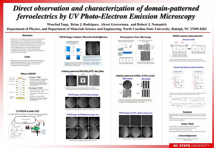
Sample (-20kV). e-beam Injection. hv. Anode (ground). positive domain. Negative domain. Positive domain. Objective lens. 1 GeV Duke Storage Ring. -. -. -. -. negative. +. Coherent FEL radiation Spontaneous Radiation 4.0-6.3eV. E. Laser Mirror. -. +. -. -. +. -. -. +.

E N D
Sample (-20kV) e-beam Injection hv Anode (ground) positive domain Negative domain Positive domain Objective lens 1 GeV Duke Storage Ring - - - - negative + Coherent FEL radiation Spontaneous Radiation 4.0-6.3eV E Laser Mirror - + - - + - - + - - + + - + + + OK-4 System Intermediate lens domain Mirror UV-XUV FEL 150oC computer & image processor Psp + Psp Psp + Psp + _ E _ UV-FEL Parameters CCD e t + + + _ Lens Column Projective lens + + + _ + + + _ Positive domain Negative domain MBE Polarization-induced bound charges • hv : 4 – 6.3 eV • Pa~ 2mW, Pp~ 20W • : 100 psec • t : 6 nsec • np : 5 x 10¹⁵ photon/sec • E/E : ~1% - + Absorbates (accumulated charges) Evaporator - + + + + + + + + + + + + + + + + + + + + + + + + AES Electrons emitted from valence band Channel Plate Psp Psp - - - - - - - - - - - - - - - - - - - - - - - - - - - - - - - - - - - - - - P-screen CCD 250oC 300oC Direct observation and characterization of domain-patterned ferroelectrics by UV Photo-Electron Emission Microscopy Woochul Yang, Brian J. Rodriguez, Alexei Gruverman, and Robert J. Nemanich Department of Physics, and Department of Materials Science and Engineering, North Carolina State University, Raleigh, NC 27695-8202 • Motivation • Precise control of ferroelectric domains has become important as a new approach to the self-assembly of complex nanostructures. • Direct information about local polarization, charge distribution, and potential of the ferroelectric surface is necessary to control the local electronic structures and to influence the chemical reactivity. • UV-FEL PEEM can allow us to image ferroelectric domain structures with high resolution (~ 10nm) and to obtain local polarization and surface electronic structures through the variation in work function on the surface. PEEM contrast of ferroelectrics PEEM Image Contrast: Photo-threshold difference Piezoresponse Force Microscopy Emission model Measure piezoelectric properties by detection of sample deformation Phase contrast of ferroelectric domain polarity Semiconductor Surfaces Minimum Escape Energy h= + Eg Evac 2 1 * 1 h 2 Eg Eg 10m • Goals • PEEM observation of ferroelectrics with polarity patterned domains • Understanding PEEM polarity contrast of ferroelectric materials • PEEM measurement of photothresholds of ferroelectrics to understand local electronic properties •Contrast between two regions can be obtained by choosing 2 < hv < 1 • Photo electrons will be emitted from region 2 (bright) but not from region 1 (dark) LNO 50m • Surface dipole induced by adsorbates changes surface electron affinity. • Electron affinity for negative domain is lower and thus emission is more intense. In phase: Brighter (negative domain) Out of phase: darker (positive domain) Ferroelectric Semiconductor Surfaces: local variations in (electron affinity), Eg(band gap), band bending, doping density will change the minimum escape energy and lead to PEEM contrast. Energy band diagram of polar domains Polarity-patterned PbZrTiO3(PZT) thin films Negative domain Eth = Eg+ s - Positive domain Eth* = Eg+ s + * What is PEEM? PEEM PFM AFM Polarity patterned LiNbO3 (LNO) crystal Evac * Concept of PEEM • Illuminate sample with UV photons just above the photoelectron threshold. • Accelerate photo-electrons with an immersion lens and image the surface with conventional electron optics with high magnification. Advantages of PEEM • Good surface sensitivity: depth(1-20 nm) • High spatial resolution: ~10nm • In situ, real-time characterization of film surfaces • Non-destructive imaging method • Measurement of surface work function and electronic structures of materials (UV-FEL PEEM) Before etching After etching Evac s eff* eff s Eth* _ Ec Eth Ec Eg PEEM AFM - EF + Eg 10m hv = 4.8eV + EF Psp - Psp Ev • In PEEM, the brightness contrast displays different polar domains. • PFM measurement confirms that the bright regions are negative domains. 10m Ev - + PFM • Difference in electron affinity due to the surface dipole causes a PEEM polarity contrast between the positive and negative end domains of ferroelectrics surfaces. • PZT - s ~ 3.5eV (Jpn. J. Appl. Phys. 38, 2272 (1999)), Eg ~ 3.4 eV Eth ~ 6.9eV - PEEM measurement: Eth ~ < 4.3eV, eff = s - = Eth – Eg = < 0.9 eV Eth* ~ > 6.0eV, eff* = s + * = Eth* – Eg = > 2.6 eV • LNO - s ~ 1.1eV (Sov. Phys. Solid State 25, 1990 (1983)), Eg ~ 3.9 eV Eth ~ 5.0 eV - PEEM measurement: Eth ~ < 4.6eV, eff = s - = Eth – Eg = < 0.7 eV Eth* ~ > 6.2eV, eff* = s + * = Eth* – Eg = > 2.3 eV + - PFM PEEM images of PZT during annealing 10m • The brighter (negative) domains is wider than darker (positive) domains. • Chemical etching (negative domain) and PFM measurement confirm that the emission from the negative domains is more intense. 10m hv = 4.9eV The polarity contrast disappears at near the Curie temperature of ~ 300oC UV-PEEM at Duke FEL • Summary • • We observed polarity contrast of domain-patterned ferroelectrics with UV-PEEM. • • Enhanced emission from negative domains is attributed to differences in electron affinity. • • The photothreshold for negative domains of LNO and PZT were found to be 4.6eV and less than 4.3eV, respectively. • Future Work • Compare PEEM of an as-loaded and clean surface of ferroelectrics • Include screening charge (internal and external) into model • XPS/UPS to measure surface Fermi level position • How are these differences manifested in other interfaces (GaN growth on PPLN) • Acknowledgements • Duke University Free Electron Laser Laboratory • ONR and AFOSR PEEM images of LNO - photon energy scan PEEM images of PZT-photon energy scan FEL-PEEM : PEEM (~10nm resolution) + FEL (tunable, high-intensity, polarized light) - + hv=4.5eV 4.6eV 4.7eV hv=4.3eV 4.8eV 5.0eV 5.2eV 5.9eV 6.2eV 6.3eV 5.2eV 5.5eV Emission threshold of negative domains is less than 4.6eV Emission threshold of negative domains is less than 4.3eV