Download
1 / 33
510 likes | 1.11k Views
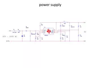
Regulated Linear Power Supply. Dual-Output Adjustable Linear Regulated Power Supply. Block Diagram. Simple Description. Transformer: “Downconvert” the AC line voltage to a smaller peak voltage Vm, usually about 2-3 Volts larger than the ultimately desired DC output.

E N D
Simple Description • Transformer: “Downconvert” the AC line voltage to a smaller peak voltage Vm, usually about 2-3 Volts larger than the ultimately desired DC output. • Diode Rectifier Circuit: produce a waveform with large DC component. • Filter: smooth out the rectified sinusoid. • Regulator: eliminate residual ripple
c03f34 Half-Wave Rectifier Tin Cause of ripple: the capacitor is discharged for almost an entire period.
c03f36 inversion Ripple Reduction: Do not allow the capacitor to discharge so frequently
An Inverting Half-Wave Rectifier If Vin >0, D1 and D2 are off. If Vin <0, D1 and D2 are on and Vout>0.
An Non-Inverting Half-Wave Rectifier If Vin >0, D1 and D2 are on, Vout>0. If Vin <0, D1 and D2 are off.
Full-Wave Rectifier Inverting Non-Inverting
Full-Wave Rectifier Alternative Drawing Full-Wave A.K.A. Bridge Rectifier Non-Inverting Inverting
Using Constant Voltage Diode Model Vout=-Vin-2VD, on Vout=Vin-2VD, on
Input versus Output |Vin|<2VD,on
Modification of Ripple Estimation Formula • Modification: • Turn-on voltage • 1/2 to account for inversion of negative • peaks.
Maximum Reverse Voltage VB=VD,on Vp is the amplitude of Vin VA=VP VAB=VP-VD,on Maximum reverse voltage is approximately Vp
Compare Maximum Reverse Bias Voltage to Half-Wave Rectifier A reverse diode voltage must sustain larger reverse bias voltage
Full-Wave Rectifier Alternative Drawing Full-Wave A.K.A. Bridge Rectifier Non-Inverting Inverting
Without Load Resistance (CL=100 uF) 9.36 V and -9.36 V
Load Assumption • Assume that the load draws 0.2 A of current • Load resistance: 9.36V/0.2A=36.5 Ohms
Each capacitor is 100 uF. Resistor is 37.5 Ohms
Increase capacitor from 100 uF to 470 uF. Reduced ripples