Download
1 / 15
150 likes | 281 Views
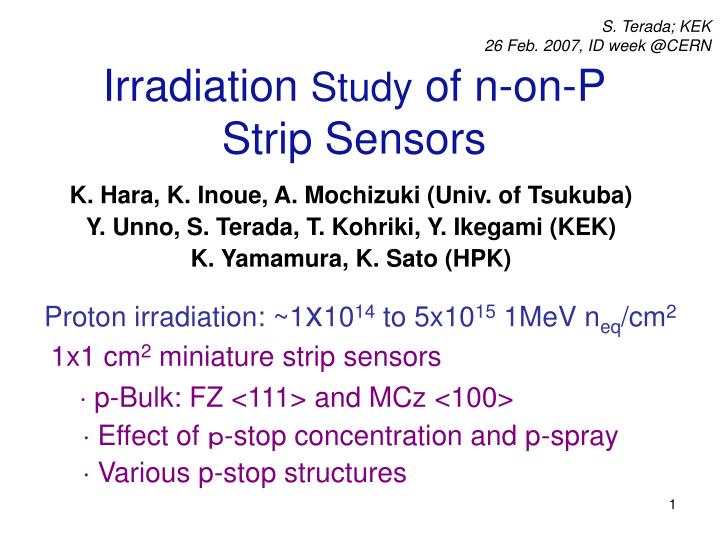
S. Terada; KEK 26 Feb. 2007, ID week @CERN. Irradiation Study of n-on-P Strip Sensors. K. Hara, K. Inoue, A. Mochizuki (Univ. of Tsukuba) Y. Unno, S. Terada, T. Kohriki, Y. Ikegami (KEK) K. Yamamura, K. Sato (HPK). Proton irradiation: ~1 x 10 14 to 5x10 15 1MeV n eq /cm 2

E N D
S. Terada; KEK 26 Feb. 2007, ID week @CERN Irradiation Study of n-on-P Strip Sensors K. Hara, K. Inoue, A. Mochizuki (Univ. of Tsukuba) Y. Unno, S. Terada, T. Kohriki, Y. Ikegami (KEK) K. Yamamura, K. Sato (HPK) Proton irradiation: ~1x10¹⁴ to 5x10¹⁵ 1MeV neq/cm2 1x1 cm2 miniature strip sensors p-Bulk: FZ <111> and MCz <100> Effect of p-stop concentration and p-spray Various p-stop structures
High resistivity 4” wafers available to HPK • p-FZ (5~10 kΩcm, <111>) • p-MCz (0.6~1 kΩcm, <100>) Strip isolation implant concentration (/cm2): p-stop only: 5x10¹², 2x10¹³ p-stop (2x10¹²) + p-splay (2x10¹²) 1x1 cm2 miniature sensors (of all above combinations) with 6 types of isolation structures (see next): 2 x 3 x 6 = 36 varieties Proton fluence (6 points): 1, 2, 5, 10, 20, 50x1014 1MeV neq/cm2
N-strip isolation structures 6 types: NS CPSTP IPSTP IPSTPDF CPSTPDF AF
Proton Irradiation at Cyclotron and Radioisotope Center (CYRIC), Tohoku University Irradiation setup • Proton beamline 31-2 • Energy: 70 MeV • Current: 10 - 500 nA • Beam spot: 4.5 mm FWHM • Samples • 3 sensors/board (10 boards stack in one run) • scanned over 20x44 mm2 for uniform irradiation • Took about 8 hours for 5x10¹⁵neq/cm2 with 350nA • fluence • dosimetry: Al activation 27Al(p,x)24Na • 1x10¹⁴ ~ 5x10¹⁵ 1 MeV-neq/cm2 Beam line
I-V :isolation structures / p-implant concentrations Pstop+Pspray Pstop 5E12 Pstop 2E13 Pre- irrad: MD more often for MCz Leakage level depends on concentration/structure but less for MCz Post- irrad: Very uniform, little dependence on concentration/structure damage constant~4x10-17 A/cm (consistent with existing data) FZ MCz 5E15 2E15 5E14 @ -20oC Pre-irrad@20oC
C-V log C vs. log V plots (f=1kHz) • Leakage current may be too much for 5E15?
Laser CCE MCz FZ 1064nm laser single shot traces @1kV Current amp PT~20ns ~5mV/fC
FDV (C-V and CCE) Summary CV and CCE agree more or less with each other (Difficult to evaluate 5E15) FZ reaches 600V at about 3E14, while MCz at 1E15 MCz higher than 600V at low fluence, below 5E13
CCE Summary not fully depleted VB=1kV 1013 1016 p-MCz: H. Hoedlmoser,RD50 workshop 06 p-DOFZ: G. Casse et al., NIMA535(2004) 362 CCE: MCz better around 0.5 - 1x10E15 Comparable to RD50 data
Conclusions and discussions Fabricated n-on-p microstrip sensors p-FZ and p-MCz wafers, with 6 types of n-strip isolation structures. p-stop implantation concentration: three values and the lowest with p-splay 1x1cm2 miniature sensors irradiated to 70-MeV protons up to 5x10¹⁵ 1MeV neq/cm2 Still have micro-discharge(MD) particularly to MCz before irradiation, however, MD goes away once irradiated FDV evaluated from C-V and laser CCE measurements p-MCz: starts at ~1kV, ~400V minimum around 2x10¹⁴/cm2, then increases to 600V at ~1x10¹⁵/cm2 p-FZ: starts at ~150V, increases rapidly and reaches to 600V at ~3x10¹⁴/cm2 Partial DV operation may be inevitable particularly to MCz at the start, unless we get higher resistivity wafer Noise studies have been under way Sensor under fabrication: 6” wafer p-FZ <100>, p-MCz <100> Next irradiation scheduled at the end of April, (then August, November and March)
Measurements of sensor characteristics I-V ・・・ micro discharge ? C-V/ CCE (Charge Collection Efficiency ) ・・・ evaluate full depletion voltage Isolation ・・・ evaluate electrical isolation between readout strips Infrared laser CCE measurement 1.5MΩ Read out 1.5MΩ 2200pF Al SiO2 IV measurement P-stop N+ N+ A A Isolation measurement LCR meter 5V P-bulk Vbias ~1.5 uA if isolated, Larger if not CV measurement Al 2200pF
Fluence evaluation by Al activation P + Al → 24Na + X Nmes : # of γ per second λ : 24Na→γ decay rate ⊿t : time from beam off to measurement Nt : # of Al atom Γ : 24Na→γ Branching ratio σ : cross section Eeff : SSD efficiency Al (6x6cm2) Al (1x1cm2) on sensor
Laser CCE setup Q-switched Nd:YAG(1064nm) laser head Intensity control (Glan polarizer+ND filters) Focusing lens Peltier cooling block with cold N2 gas outlets (-20oC) Reference sample Amplifier box Current amp (PT=20ns) Laser position monitor