Download
1 / 24
240 likes | 470 Views
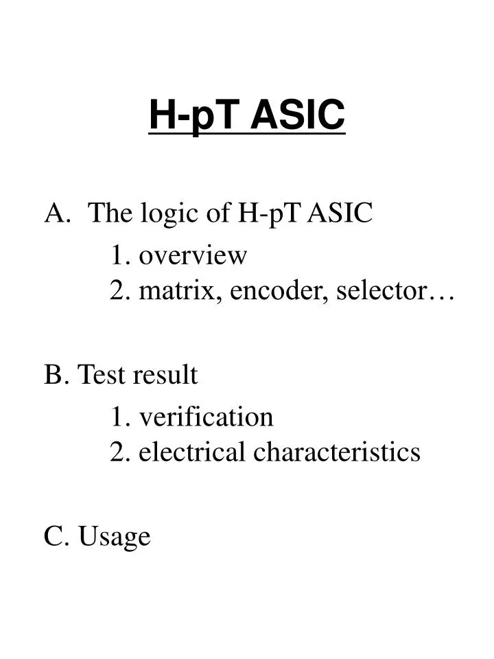
H-pT ASIC. The logic of H-pT ASIC 1. overview 2. matrix, encoder, selector… B. Test result 1. verification 2. electrical characteristics C. Usage. Setting of High-pT ASIC and boards. G-LINK Optical. PP. ASD. LVDS. SL. HPT. PS. LVDS.

E N D
H-pT ASIC • The logic of H-pT ASIC 1. overview 2. matrix, encoder, selector… B. Test result 1. verification 2. electrical characteristics C. Usage
Setting of High-pT ASIC and boards G-LINK Optical PP ASD LVDS SL HPT PS LVDS Block diagram of end-cap muon level-1 trigger system
Primary selector encoder sub matrix unit High-pT ASIC Block Diagram triplet in delay control triplet-decoder 6 to 2 selector doublet-decoder output A sub matrix unit delay control doublet in H/L selector 6 to 2 selector output B
triplet in Selecting the highest pT hit corresponding to centered one doublet in Primary selector encoder sub matrix unit Selecting highest 2 hits If the same pT, ASIC chooses upper one. 6 to 2 selector sub matrix unit H/L Selector H has 1st priority, pT is 2nd priority. HHLL=HH HLL=HL LL=LL From HpT 6 to 2 sel H/L selector From LpT 6 to 2 sel
001 0 1 010 011 position (oxpos) 100 101 hit ID (oxid) 110 Output Data Format primary output secondary output 1:HpT 0:LpT No hit = 0 0000 -1 = 0 0001 +1 = 1 0001 -2 = 0 0010 for example triplet 0 60 000 = no hit 54 0 doublet
ASIC Control Signal 000000 101010 LVDS Serializer invsw=1 - - - 0 1 0 1 1 dset 1 0 1 1 0 1
Delay Control 3bit delay controlled by JTAG or VME This ASIC has 3bit X 7 delay for 7 blocks. From triplet From doublet wire mode 2 way setting method of delay registers JTAG : dj=1, data from JTAG VME : dj=0, data from VME, set by dset @ 0.5CLK
JTAG Register y=0 mode will be used in read-back. Delay Block2 TDI TDO
All the registers of H-pT ASIC are voting structure SEU XOR IN MAJ OUT If there is a SEU on a register, we can detect with SEU-pin. example OUT SEU 1 1 1 1 0 1 0 1 1 1 1 0 0 0 1
Costs for mass-production of H-pT ASIC \2,550 = € 21.74 = 31.89CHF @chip Geometry Ball Grid Array 256-pins
# of input pin 54 (doublet-in) 60 (triplet-in) 3 (TDI, TMS, TCK) 2 (clk, reset) 21 (delay control) 5 (inv, or, ws, dset, dj) total 145 # of output pin 10 (A-out) 10 (B-out) 1 (SEU) 1 (TDO) 3 (for g-link control) total 25 Pin spec. of H-pT ASIC
Test Setup for verification test PPG50 (Pattern Gen) TOM (FIFO) LVTTL LVTTL HPT Test Board Test bit-pattern compare PC PPG50 = pattern generator ROD = output-data storage PC = simulator and comparator
Checking List Matrix Verification wire strip Delay ASIC Control (dc, reset, or, w/s, dj, dset)
Test Setup for connection test Trigger System Hardware Test bit-pattern compare Trigger System Simulation Checking List JTAG Control
Timing Characteristics setup/hold time iclk Input data <1.0 <1.0ns typical delay iclk data Outgoing data 32 < td < 34 ns 33ns << 3clocks (TDR)
Electrical Characteristics * Limited by test system, PPG50
For the wire board Optical OUT EO-CONV HpT ASIC LVDS Rx G-LINK LVDS IN Optical OUT For the Strip board EO-CONV HpT ASIC LVDS Rx G-LINK TC7MA157FK LVDS IN Output Format if pT > 0, OUT = no hit
EWD 1 EWD 2 EWD 3 EWT 1 EWT 2 EWD 4 EWD 5 EWD 6 EWT 3 EWT 4 EWD 7 EWD 8 EWD 9 Sector Logic Sector Logic Sector Logic Sector Logic EWT 5 EWT 6 High-pT Board (Endcap-Wire) 9U-VME BOARD EWD 0 HPt ASIC EWT 0 VME operation G HPt ASIC G HPt ASIC G HPt ASIC Clock, JTAG, and reset G LVDS Rx Optical Fiber Doublet 18-bit → serialized LVDS Triplet 18-bit → serialized LVDS
ESD3 ’ ESD4 ’ EST1 ’ High-pT Board (Endcap-Strip) 9U-VME BOARD Sector Logic ESD0 ESD1 ESD2 G HPt ASIC VME operation Sector Logic EST0 G ESD3 ESD4 HPt ASIC Sector Logic EST1 ESD0 ‘ ESD1 ‘ ESD2 ‘ G HPt ASIC Sector Logic EST0 ’ G Clock, JTAG, and reset HPt ASIC TC7MA157FK LVDS Rx Optical Fiber Doublet 18-bit → serialized LVDS Triplet 2x20-bit → serialized LVDS
High-pT Board (Forward) 9U-VME BOARD Sector Logic FWD0 FWD1 FWD2 G HPt ASIC VME operation FWT0 FWT1 Sector Logic G FWD3 HPt ASIC FWT2 FWT3 Sector Logic G HPt ASIC FSD0 Clock, JTAG, and reset FST0 HPt ASIC TC7MA157FK LVDS Rx Optical Fiber Doublet 18-bit → serialized LVDS Triplet 18/20-bit → serialized LVDS
SUMMARY • All the functions of H-pT ASIC have been verified. • The electrical characteristics have been checked. • We have designed 3 H-pT boards available