Download
1 / 17
190 likes | 676 Views
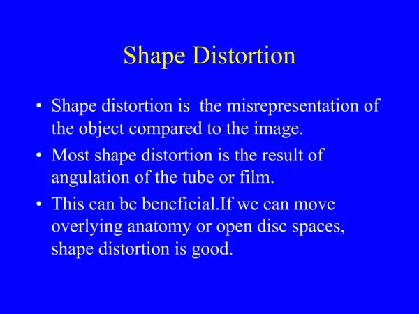
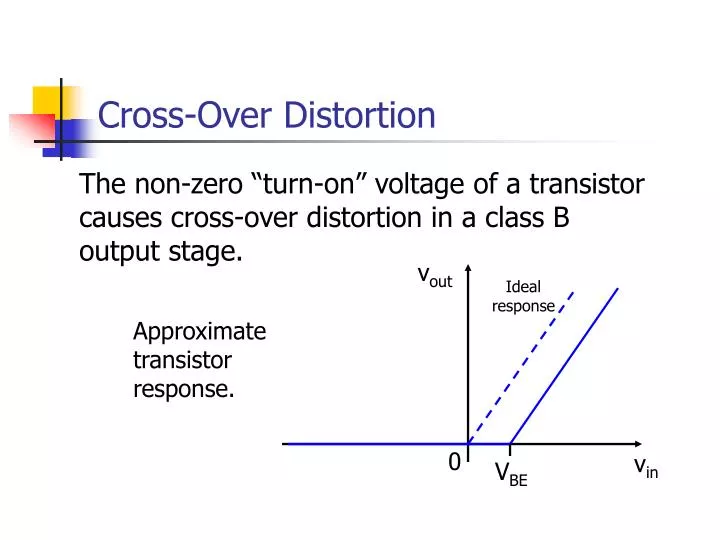
Ideal response. Cross-Over Distortion. The non-zero “turn-on” voltage of a transistor causes cross-over distortion in a class B output stage. v out. Approximate transistor response. 0. v in. V BE. NPN response for v B = v IN +0.7. NPN response. PNP response.

E N D
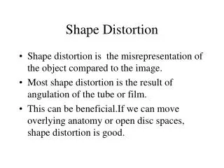
Ideal response Cross-Over Distortion The non-zero “turn-on” voltage of a transistor causes cross-over distortion in a class B output stage. vout Approximate transistor response. 0 vin VBE
NPN response for vB = vIN+0.7 NPN response PNP response PNP response for vB = vIN-0.7 Eliminating Cross-Over Distortion vout vin
Eg. Positive half cycle: Class AB Output Stage
Practical Class AB Stages • In practice, there isn’t an exact “turn-on” voltage (VBE). • Vbias is set slightly high so that there is a non-zero quiescent collector current. • Each transistor will now conduct for slightly more than 180° - i.e. Class AB operation.
Class AB Efficiency • Slightly more power is dissipated using a class AB stage compared with a class B due to the non-zero quiescent collector current. • In a well designed circuit, this extra power should be insignificant so the class B efficiency calculations are still valid. • I.e. maximum efficiency = 78 %.
Net result is that if VBE is fixed, IC rises exponentially with temperature. Thermal Effects The quiescent collector current depends on VBE and also on the junction temperature. So, in designing the biasing network, thermal effects must be considered.
Thermal Effects 1.2 0.8 Collector Current [mA] (VBE=0.5 V) 0.4 0 20 30 40 50 60 Temperature [°C]
Temperature rises Collector current rises Power dissipation increases Thermal Runaway Collector Current Flows, so power is dissipated
Suppressing Thermal Runaway • Fit a bigger heatsink. • Use series emitter-resistors. • Use a temperature dependent bias voltage. • The latter two are preferred methods. Both introduce negative feedback.
By symmetry: Emitter Resistors So, if IC rises, VBE falls and IC is reduced. Note RE should be small compared with RL to minimise power wasted.
Base current is negligible, so: VBE Bias Voltage – The VBE Multiplier
VBE Multiplier – Temperature Effects • If junction temperature rises but IC stays the same, VBE must fall causing Vbias to fall also. • Negative thermal feedback achieved if the transistor is in close contact with the output devices. • Especially suitable for integrated circuits where close thermal contact is guaranteed.
Design Example – (i) RE Let RL = 16 W and Amax = 12 V. (Also assume Vout = 0 through d.c. feedback).
Design Example – (ii) Ibias NB. Ibias is set well above minimum to ensure that a significant current flows through the VBE multiplier.
Design Example – (iii) Vbias Peak output current = 0.75 A, choose quiescent collector current to be small by comparison, e.g.
For constant bias voltage, Design Example – (iii cont) Vbias
Class AB – Summary • Class AB achieves the efficiency of a class B output stage but without cross-over distortion. • Biasing arrangements are more complex, however, as the threat of thermal runaway must be eliminated.