Download
1 / 24
270 likes | 466 Views
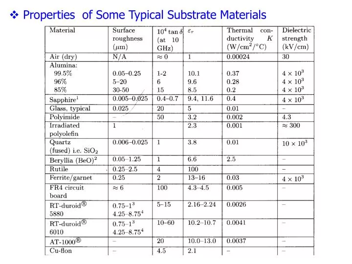
Properties of Some Typical Substrate Materials. MIC Manufacturing Technology. Thin-Film Module. Circuit is accomplished by a plate-through technique or an etch-back technique. Thick-Film Module. 1) Thick-film patterns are printed and fired on the ceramic substrate.

E N D
MIC Manufacturing Technology • Thin-Film Module • Circuit is accomplished by a plate-through technique or an etch-back technique. • Thick-Film Module 1) Thick-film patterns are printed and fired on the ceramic substrate. 2) Printed circuit technique is used to etch the desired pattern in a plastic substrate. • Medium-Film Module • Above technologies are suitable for HMIC productions. • Monolithic Technology • This technology is suitable for MMIC productions.
Multi-Chip Modules (MCM) • MCM provides small, high precision interconnects among multiple ICs to form a cost-effectively single module or package. • Four dominant types of MCM technologies: 1) MCM-L having a laminated PCB-like structure. 2) MCM-C based on co-fired ceramic structures similar to thick-film modules. 3) MCM-D using deposited metals and dielectrics in a process very similar to that used in semiconductor processing. 4) MCM-C/D having deposited layers on the MCM-C base • Advantages of an MCM over a PCB are : 1) Higher interconnect density. 2) Finer geometries enables direct chip connect. 3) Finer interconnect geometries enables chips placed closer together and it results in shorter interconnect lengths.
Low Frequency Characters of Microstrip Line
Microstrip Line • Microstrip line is the most popular type of planar transmission lines, primarily because it can be fabricated by photolithographic processes and is easily integrated with other passive and active RF devices. • When line length is an appreciable fraction of a wavelength (say 1/20th or more), the electric requirements is often to realize a structure that provides maximum signal, or power, transfer. • Example of a transistor amplifier input network • Microstrip components • Transmission line • Discontinuities • Step • Mitered bend • Bondwire • Via ground
The most important dimensional parameters are the microstrip width w, height h (equal to the thickness of substrate), and the relative permittivity of substrate r. • Useful feature of microstrip : • DC as well as AC signals may be transmitted. • Active devices and diodes may readily be incorporated. • In-circuit characterization of devices is straightforward to implement. • Line wavelength is reduced considerably (typically 1/3) from its free space value, because of the substrate fields. Hence, distributed component dimensions are relatively small. • The structure is quite rugged and can withstand moderately high voltages and power levels. • Although microstrip has not a uniform dielectric filling, energe transmission is quite closely resembles TEM; it’s usually referred to as ‘quasi-TEM’.
Electromagnetic Analysis Using Quasi-Static Approach (Quasi-TEM Mode) • The statically derived results are quite accurate where frequency is below a few GHz. • The static results can still be used in conjunction with frequency-dependent functions in closed formula when frequency at higher frequency. • Characteristic Impedance Z0 For air-filled microstrip lines, For low-loss microstrip lines, We can derive
w er h w er h Procedure for calculating the distributed capacitance: • Effective Dielectric Constant e For very wide lines, w / h >> 1 For very narrow lines, w / h << 1
We can express eeff as where filling factor qrepresents the ratio of the EM fields inside the substrate region, and its value is between ½ and 1. Another approximate formula for q is (provided by K.C. Gupta, et. al.) • Planar Waveguide Model (Parallel-Plate Model)
Conductor Lossac • In most microstrip designs with high r, conductor losses in the strip and ground plane dominate over dielectric and radiation losses. • It’s a factors related to the metallic material composing the ground plane and walls, among which are conductivity, skin effect, and surface roughness. • Relationships: • Dielectric Lossad • To minimize dielectric losses, high-quality low-loss dielectric substrate like alumina, quartz, and sapphire are typically used in HMICs. • In MMICs, Si or GaAs substrates result in much larger dielectric losses (approximately 0.04 dB/mm).
Radiation Loss ar • Radiation loss is major problem for open microstrip lines with low . Lower (5) is used when cost reduction is a priority, but it lead to radiation loss increased. • The use of top cover and side walls can reduce radiation losses. Higher substrate can also reduce the radiation losses, and has a benefit in that the package size decreases by approximately the square root of . This benefit is an advantage at low frequency, but may be a problem at higher frequencies due to tolerances.
Formulations of Attenuation Constant a However, the dielectric loss should occur in the substrate region only, not the whole region. Therefore, ad should be modified as
How to evaluate attenuation constant • Method 1 : in Chapter 2.14 ; is calculated from RLCG values of material. • Method 2: Perturbation method where Plis power loss per unit length of line, P0is the power on line at z=0 plane. • Method 3: is calculated from material parameters. where ac is attenuation due to conductor loss ad is attenuation due to dielectric loss ar is attenuation due to radiation loss • Combined Loss Effect : linearly combined quality factors (Q)
Recommendations • Use a specific dimension ratio to achieve the desired characteristic impedance. Following that, the strip width should be minimized to decrease the overall dimension, as well as to suppress higher-order modes. However, a smaller strip width leads to higher losses. • Power-handling capability in microstrip line is relatively low. To increase peak power, the thickness of the substrate should be maximized, and the edges of strip should be rounded ( EM fields concentrate at the sharp edges of the strip). • The positive effects of decreasing substrate thickness are : • Compact circuit • Ease of integration • Less tendency to launch higher-order modes or radiation • The via holes drilled through dielectric substrate contributing smaller parasitic inductances However, thin substrate while maintaining a constant Z0 must narrow the conductor width w, and it consequently lead to higher conductor losses, lower Q-factor and the problem of fabrication tolerances.
Using higher substrate can decrease microstrip circuit dimensions, but increase losses due to higher loss tangent. Besides, narrowing conductor line have higher ohmic losses. Therefore, it is a conflict between the requirements of small dimensions and low loss. For many applications, lower dielectric constant is preferred since losses are reduced, conductor geometries are larger ( more producible), and the cutoff frequency of the circuit increases. For microwave device applications, microstrip generally offers the smallest sizes and the easiest fabrication, but not offer the highest electrical performance.
Design a microstrip line by the method of • “Approximate Graphically-Based Synthesis”
Example1: Design a 50 microstrip line on a FR4 substrate( r=4.5). Solution Assume eff= r=4.5 From Zo1 curve w/h=1.5 From q-curve q=0.66 eff= 1+q(r+1)=1+0.66(4.5-1)=3.31 • 2nd iteration eff= 3.31 From Zo1 curve w/h=1.7 From q-curve q=0.68 eff= 1+q(r+1)=1+0.68(4.5-1)=3.38 • 3rd iteration • Stable result w/h=1.88; eff=3.39
Formulas for Quasi-TEM Design Calculations • Analysis procedure: Give w / h to find eeff and Z0. (provided by I.J. Bahl, et. al.) • Synthesis procedure: Give Z0 to find w / h.
Example2: Calculate the width and length of a microstrip line for a 50 Characteristic impedance and a 90° phase shift at 2.5 GHz. The substrate thickness is h=0.127 cm, with eff=2.20. Solution Guess w/h>2 Matched with guess Then w=3.081h=0.391 (cm) The line length, l, for a 90° phase shift is found as
Microstrip on an Dielectrically Anisotropic Substrate Empirical formula
Curve : i=10.6 ; Curve : used reqformula