Download
1 / 55
550 likes | 683 Views
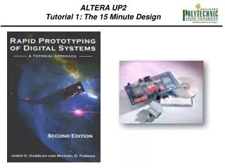
ALTERA UP2 Tutorial 1: The 15 Minute Design. ALTERA UP2 Tutorial 1: The 15 Minute Design. Figure 1.1 The Altera UP 1 CPLD development board. ALTERA UP1: Chapter 5 Core Library Functions. ALTERA UP1: Chapter 5 Core Library Functions. Figure 5.1 Symbol for DEC_7SEG UP1core.

E N D
ALTERA UP2Tutorial 1: The 15 Minute Design Figure 1.1 The Altera UP 1 CPLD development board.
ALTERA UP1: Chapter 5Core Library Functions Figure 5.1 Symbol for DEC_7SEG UP1core.
ALTERA UP1: Chapter 5Core Library Functions Figure 5.2 Symbol for DEBOUNCE UP1core.
ALTERA UP1: Chapter 5Core Library Functions Figure 5.3 Symbol for ONEPULSE UP1core.
ALTERA UP1: Chapter 5Core Library Functions Figure 5.4 Symbol for CLK_DIV UP1core.
ALTERA UP1: Chapter 5Core Library Functions Figure 5.5 Symbol for VGA_SYNC UP1core.
ALTERA UP1: Chapter 5Core Library Functions Figure 5.6 Symbol for CHAR_ROM UP1core.
ALTERA UP1: Chapter 5Core Library Functions Figure 5.7 Symbol for KEYBOARD UP1core.
ALTERA UP1: Chapter 5Core Library Functions Figure 5.8 Symbol for MOUSE UP1core.
LIBRARYIEEE; -- Include Libraries for standard logic data types USEIEEE.STD_LOGIC_1164.ALL; -- Entity name normally the same as file name ENTITY gate_network IS -- Ports: Declares module inputs and outputs PORT( A, B, C : INSTD_LOGIC; -- Standard Logic Vector ( Array of 4 Bits ) D : INSTD_LOGIC_VECTOR( 3 DOWNTO 0 ); -- Output Signals X, Y : OUTSTD_LOGIC ); END gate_network; -- Defines internal module architecture ARCHITECTURE behavior OF gate_network IS BEGIN -- Concurrent assignment statements operate in parallel -- D(1) selects bit 1 of standard logic vector D X <= A ANDNOT( B OR C ) AND ( D( 1 ) XOR D( 2 ) ); -- Process must declare a sensitivity list, -- In this case it is ( A, B, C, D ) -- List includes all signals that can change the outputs PROCESS ( A, B, C, D ) BEGIN -- Statements inside process execute sequentially Y <= A ANDNOT( B OR C) AND ( D( 1) XOR D( 2 ) ); ENDPROCESS; END behavior;
ENTITY hierarch ISPORT ( clock_25Mhz, pb1 : INSTD_LOGIC; pb1_single_pulse : OUTSTD_LOGIC);END hierarch;ARCHITECTURE structural OF hierarch IS-- Declare internal signals needed to connect submodulesSIGNAL clock_1MHz, clock_100Hz, pb1_debounced : STD_LOGIC;COMPONENT debounce -- Use Components to Define Submodules and ParametersPORT( pb, clock_100Hz : INSTD_LOGIC; pb_debounced : OUTSTD_LOGIC);ENDCOMPONENT; COMPONENT onepulsePORT(pb_debounced, clock : INSTD_LOGIC; pb_single_pulse : OUTSTD_LOGIC);ENDCOMPONENT;COMPONENT clk_divPORT( clock_25Mhz : INSTD_LOGIC; clock_1MHz : OUTSTD_LOGIC; clock_100KHz : OUTSTD_LOGIC; clock_10KHz : OUTSTD_LOGIC; clock_1KHz : OUTSTD_LOGIC; clock_100Hz : OUTSTD_LOGIC; clock_10Hz : OUTSTD_LOGIC; clock_1Hz : OUTSTD_LOGIC);ENDCOMPONENT; BEGIN-- Use Port Map to connect signals between components in the hierarchydebounce1 : debounce PORTMAP ( pb => pb1, clock_100Hz = >clock_100Hz, pb_debounced = >pb1_debounced);prescalar : clk_div PORTMAP ( clock_25Mhz = >clock_25Mhz, clock_1MHz =>clock_1Mhz, clock_100hz = >clock_100hz);single_pulse : onepulse PORTMAP ( pb_debounced = >pb1_debounced, clock => clock_1MHz, pb_single_pulse => pb1_single_pulse);END structural;
ALTERA UP1: Chapter 6VHDL of Synthesis of Digital Hardware Figure 6.3 Using a Testbench for automatic verfication
Figure 7.1 Track Layout with Input Sensors and Output Switches and Output Tracks.
D A = 0 1 : S u p p l y A F o r w a r d T 1 = 0 : T r a c k 1 s e t t o S u p p l y A S w i t c h 3 T r a c k 1 T r a c k 3 S e n s o r 5 S e n s o r 1 S e n s o r 2 S e n s o r 3 S e n s o r 4 T r a c k 4 T r a c k 2 S w i t c h 1 S w i t c h 2 Figure 7.3 Track Power is connected to one of Two Power Sources: A and B.
Figure 7.4 Track Direction if all Switches are Asserted (SW1 = SW2 = SW3 = 1)
Figure 7.8 Working diagrams of train positions for each state.