Download
1 / 18
190 likes | 339 Views
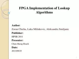
FPGA Implementation of RC6 including key schedule. Hunar Qadir Fouad Ramia. Introduction. RC6 is a symmetric key block cipher derived from RC5 One of the five finalists chosen for AES Works on a block size of 128 bits Specified as RC6- w/r/b Supports key sizes of 64, 128, and 256 bits.

E N D
FPGA Implementation of RC6 including key schedule Hunar Qadir Fouad Ramia
Introduction • RC6 is a symmetric key block cipher derived from RC5 • One of the five finalists chosen for AES • Works on a block size of 128 bits • Specified as RC6-w/r/b • Supports key sizes of 64, 128, and 256 bits
Goal of our project • Implementation of RC6 in hardware • FPGA as the target technology • Implementation of key schedule/generator in addition to encryption/decryption • Study/compare the performance of our design
Motivation • Why RC6? • Security • Simplicity • Performance • Why FPGAs? • Higher performance than software solutions • Reprogrammable (FPGA vs. ASICs)
RC6 Algorithm • Key Schedule • User supplies a key of b bytes • 2r + 4 words (w bits each) are derived and stored in the array S [0, 2r + 3] • Array is used in both encryption and decryption
RC6 Algorithm (continued) • Encryption • Plain text stored in four w-bit input registers A, B, C, D B = B + S [0] D = D + S [1] for i = 1 to r do { T = (B X (2B + 1)) <<< lg w u = (D X (2D + 1)) <<< lg w A = ((A t) <<< u) + S [2i] C = ((C u) <<< t) + S [2i+ 1] (A, B, C, D) = (B, C, D, A) } A = A + S [2r + 2] C = C + S [2r + 3] *Figure taken from RC6 paper by Ron Rivest
RC6 Algorithm (continued) • Decryption • Cipher text stored in four w-bit input registers A, B, C, D C = C – S [2r + 3] A = A – S [2r + 2] for i = r downto 1 do { (A, B, C, D) = (D, A, B, C) u = (D X (2D + 1)) <<< lg w t = (B X (2B + 1)) <<< lg w C = ((C – S [2i + 1]) >>> t) u A = ((A – S [2i]) >>> u) t } D = D – S [1] B = B – S [0]
Development Environment • Use VHDL to simulate hardware implementation • CAD tools used: • ALDEC Active HDL • Synplify Pro 8.5 for synthesis • Xilinx ISE 7.1 for implementation • Selection of a target FPGA • Xilinx Virtex XCV1000
Implementation results • Min. Period (ns) : • 22.881 • Max. Frequency (MHz) : • 43.7 • Throughput Including key generation • 27 Mbit/sec • Throughput Encryption/Decryption only • 266 Mbit/sec
Conclusion & Future Work • Pros and Cons of Key Schedule on board • Future Work: Compute round keys on the fly