Download
1 / 2
30 likes | 52 Views
Wafer World is not only a thought leader in the wafer semiconductor, we are also one of the premier manufacturers and distributors in the business. Purchase our Wafers today at sales@waferworld.com.

E N D
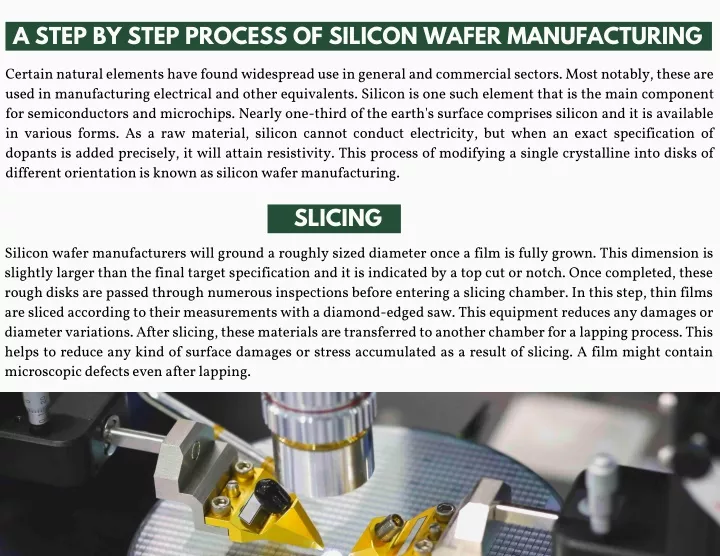
A STEP BY STEP PROCESS OF SILICON WAFER MANUFACTURING Certain natural elements have found widespread use in general and commercial sectors. Most notably, these are used in manufacturing electrical and other equivalents. Silicon is one such element that is the main component for semiconductors and microchips. Nearly one-third of the earth's surface comprises silicon and it is available in various forms. As a raw material, silicon cannot conduct electricity, but when an exact specification of dopants is added precisely, it will attain resistivity. This process of modifying a single crystalline into disks of different orientation is known as silicon wafer manufacturing. SLICING Silicon wafer manufacturers will ground a roughly sized diameter once a film is fully grown. This dimension is slightly larger than the final target specification and it is indicated by a top cut or notch. Once completed, these rough disks are passed through numerous inspections before entering a slicing chamber. In this step, thin films are sliced according to their measurements with a diamond-edged saw. This equipment reduces any damages or diameter variations. After slicing, these materials are transferred to another chamber for a lapping process. This helps to reduce any kind of surface damages or stress accumulated as a result of slicing. A film might contain microscopic defects even after lapping.
INGOT GROWTH Certain natural elements have found widespread use commercial sectors. Most notably, these are used in manufacturing electrical and other equivalents. Silicon is one such element that is the main component for semiconductors and microchips. Nearly one-third of the earth's surface comprises silicon and it is available in various forms. As a raw material, silicon cannot conduct electricity, but when an exact specification of dopants precisely, it will attain resistivity. This process of modifying a single crystalline into disks of different orientation is known as silicon wafer manufacturing. in general and is added CLEANING The final and most crucial step of this process is cleaning. It is performed in two or three stages with different modalities. At first, cleaning in a vacuumed chamber removes a thin layer of material from finished disks. This is essential to achieve a precise dimension. The next two stages don’t involve any removal rather than a long bathing process. It also polishes the surface for achieving a mirror finish that is used during device fabrications.