Download
1 / 3
30 likes | 131 Views
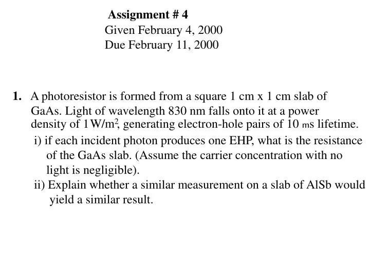
Assignment # 4. Given February 4, 2000 Due February 11, 2000. 1. A photoresistor is formed from a square 1 cm x 1 cm slab of GaAs. Light of wavelength 830 nm falls onto it at a power density of 1 , generating electron-hole pairs of 10 m s lifetime.

E N D
Assignment # 4 Given February 4, 2000 Due February 11, 2000 1. A photoresistor is formed from a square 1 cm x 1 cm slab of GaAs. Light of wavelength 830 nm falls onto it at a power density of 1 , generating electron-hole pairs of 10 ms lifetime. i) if each incident photon produces one EHP, what is the resistance of the GaAs slab. (Assume the carrier concentration with no light is negligible). ii) Explain whether a similar measurement on a slab of AlSb would yield a similar result. W/m2
2. • A Hall effect measurement is made on a semiconductor sample with • length 0.5 cm, width 0.2 cm, and cross-sectional area of 10-2cm2. • With a constant current supply, 0.4 mA flow through the length of • the sample. Determine: • The resistivity of the sample if the potential Vx across the length • of the sample is 1.0 V. • The carrier type. A magnetic field of 0.75 T is applied normal to • the sample, and a Hall voltage VH = 0.1 V is measured (across the • width with polarity as indicated). - see next page -
Question 2 cont’d: • The carrier concentration. • The carrier mobility. • The values of Vx and VH if the carrier concentration is doubled. For Si that is very lightly doped with NA=3.71010cm-3, calculate the equilibrium electron and hole concentrations ( ni = 1.51010cm-3 , T = 300K ). Find the displacement of the Fermi energy level EF from the band gap position. 3. Note: You can use 4. Problem 3.10, p 93, textbook, 4th edition