Download
1 / 15
150 likes | 221 Views
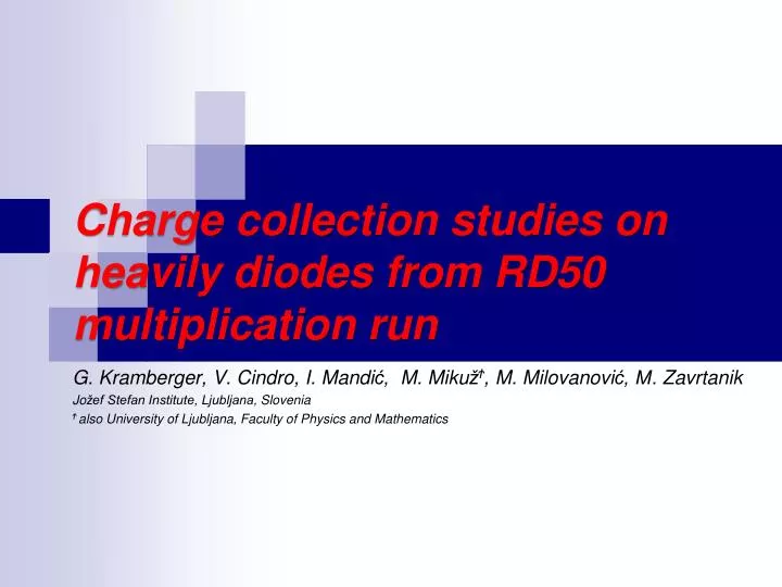
Charge collection studies on heavily diodes from RD50 multiplication run . G. Kramberge r , V. Cindro, I. Mandi ć, M. Mi ku ž Ϯ , M. Milovanovi ć, M . Zavrtanik Jo žef Stefan Institute, Ljubljana, Slovenia Ϯ also University of Ljubljana, Faculty of Physics and Mathematics.

E N D
Charge collection studies on heavily diodes from RD50 multiplication run G. Kramberger, V. Cindro, I. Mandić, M. MikužϮ, M. Milovanović, M. Zavrtanik Jožef Stefan Institute, Ljubljana, Slovenia Ϯ also University of Ljubljana, Faculty of Physics and Mathematics
Motivation RD50 had/has a “multiplication wafer” run with Micron, which included special devices/diodes for studying: • Impact of various parameters on charge multiplication • Does implant diffusion time matter? • Does energy of implantation ions matter? • How much does thickness matter? • What is the wafer-to-wafer reproducibility? G. Kramberger, Charge collection studies on heavily diodes from RD50 multiplication run,20th RD50 Workshop, Bari, 2012
Samples • Special diodes-pad detectors were designed on that wafers which are particularly suitable for studies of charge collection: • DC coupled, guard ring structure – high breakdown voltage • 80 mm pitch, 20 mm implant width • 4x4 mm2 , 300 and 150 mm thick • All strips connected together at one side: • almost the same electric field as in strip detector • much simpler handling (CCE, CV-IV etc measurements) • weighting field similar to that of a diode Type 3 (used in this work) Metalized implant Type 2: Not-metalized implant Type 1: Partially metalized implant G. Kramberger, Charge collection studies on heavily diodes from RD50 multiplication run,20th RD50 Workshop, Bari, 2012
Tex2440 Amplifier +shaper pad detector 90Sr/241Am thermal isolation cold plate scintillator Peltier cooler water cooled heat sink Irradiations and measurements Type 3: samples from different wafers: 2935-2– standard 2e15 cm-2, 150 keV P 2935-3- standard 5e15 cm-2, 80 keVB 2935-4– standard 220 nm thermal oxide 2935-5 - standard 2935-6 - standard 2935-7 – standard 2935-8 - standard 2935-9 – standard 2884-7 – standard 2935-10 - double diffusion (1000oC for 3h) 2912-2 - double energy 300 keV of P ions 2912-3 - double energy doubly charged ! 2885-5 – thin • Sample treatment: • Neutron irradiations: 3∙1015 cm-2 and 1016 cm-2 • Measurements done at -20ºC for 3∙1015 cm-2 and -23oC (1016 cm-2) • Irradiation performed in steps with 80 min annealing at 60oC in between • 3samples were irradiated in a single step also to1015 cm-2, 2∙1015cm-2 and 1016cm-2 to check the consistency • Measurements: • CCE measurements with 90Sr setup • 25 ns shaping • 98% trigger purity • Calibrated for non-irradiated detector with 59.5 keV line from 241Am • CV at RT for non-irradiated samples • IV for cold and irradiated samples G. Kramberger, Charge collection studies on heavily diodes from RD50 multiplication run,20th RD50 Workshop, Bari, 2012
Capacitance and current characteristics Standard thickness: C~6 pF (thick), C~12 pF (thin), Vfd~70 V (~40 V for thin). 1/C2 vs. Vbias deviates from straight line for some samples Current are around 10 nA at full depletion voltage. Only one sample showed a soft breakdown. G. Kramberger, Charge collection studies on heavily diodes from RD50 multiplication run,20th RD50 Workshop, Bari, 2012
CCE and noise for non-irradiated samples without detector ENC~2000 e variation of ~10% for charge at V>Vfd – several samples were re-measured and reproducibility was found to be better than that good agreement of Vfddetermined from Q-V with that of C-V Noise performance in accordance with expectations G. Kramberger, Charge collection studies on heavily diodes from RD50 multiplication run,20th RD50 Workshop, Bari, 2012
CCE (I) - wafer to wafer reproducibility 1016 cm-2 3∙1015 cm-2 • Wafer-wafer (randomly chosen samples) variation of CCE is within 10% (peak-peak) – comparable or better than before the irradiation. • Larger problem with micro discharges for lower fluence. Radiation improves HV stability significantly – no problem of operation all samples at >1000 V. • Linear rise of MPC with voltage – deviation at larger bias – multiplication? • Degradation of CCE as expected from previous measurements. G. Kramberger, Charge collection studies on heavily diodes from RD50 multiplication run,20th RD50 Workshop, Bari, 2012
CCE (II) - implantation and thickness 1016 cm-2 (double energy) (double diffusion) (thin) 3∙1015 cm-2 • almost no difference in charge collection efficiency for different implants (… but only limited parameter region of investigation, see I. Mandic talk where it is shown that implants should play a role) • dQ/dV(3e15)/dQ/dV(1e16)~2.5 • Large difference between thick and thin detectors: • very high CCE for thin detector (~10-11 ke for 3∙1015 cm-2). • up to 1000 V thin are at least as good as thick • only moderate increase of charge collection with high bias voltages for thin device – why don’t we see larger increase of multiplication? G. Kramberger, Charge collection studies on heavily diodes from RD50 multiplication run,20th RD50 Workshop, Bari, 2012
Leakage current performance scaled to -20oC for 1016 cm-2 volume generation current 1016 cm-2 3∙1015 cm-2 thin sample …, but the Ileak is a sum of guard and bulk currents Leakage current larger than given by volume bulk does not scale precisely with fluence (factor ~3) – difference in MI ? G. Kramberger, Charge collection studies on heavily diodes from RD50 multiplication run,20th RD50 Workshop, Bari, 2012
Noise performance micro discharges increase of noise with bias is smaller than increase of signal with bias Thin detector has larger noise, but only marginally similar noise for low and high fluence measurements although leakage current differ by factor of 2 – () G. Kramberger, Charge collection studies on heavily diodes from RD50 multiplication run,20th RD50 Workshop, Bari, 2012
Fluence dependence of CCE Solid markers – spaghetti diodes Open markers – strip detectors Samples irradiated to fixed fluences and annealed for 80 min @ 60oC • Larger charge collection for strip detectors can be attributed to more favorable weighting field profile and difference in absolute charge calibration • ~15% difference at 1100 V for 3∙1015 cm-2, ~30% difference for 1016cm-2 • Larger fraction of weighting potential is in the region with very high electric field G. Kramberger, Charge collection studies on heavily diodes from RD50 multiplication run,20th RD50 Workshop, Bari, 2012
CCE – beneficial annealing • Around 30% better charge collection efficiency as before annealing • Much larger CCE for spaghetti diode than for standard RD50 diode from previous Micron run: • the effect of multiplication, due to strip geometry? • partially also weighting field? - although only a small difference in the between standard and spaghetti diode G. Kramberger, Charge collection studies on heavily diodes from RD50 multiplication run,20th RD50 Workshop, Bari, 2012
CCE – irradiation in steps How does the irradiation in steps with subsequent annealing compare to fixed fluence irradiation? Almost identical most probable charge measured! G. Kramberger, Charge collection studies on heavily diodes from RD50 multiplication run,20th RD50 Workshop, Bari, 2012
Conclusions & future work • New “spaghetti” diodes perform well • Within the parameter space investigated in RD50 Micron Multiplication run: • the “double energy” of implantation ions and • the “double diffusion time” processed diodes perform equally for charge collection measurements with 90Sr electrons as standard diodes • Thin diodes perform better than standard ones for both fluences up to 1000 V • The “CERN scenario” irradiations give identical results as samples irradiated to fixed fluences and subsequently annealed at RT for 14 day • As expected the spaghetti diodes perform “better” than standard diodes and worse than strip detectors at given fluence, annealing time and voltage due to difference in weighting field. Further studies are underway with TCT for which these samples are ideal ! G. Kramberger, Charge collection studies on heavily diodes from RD50 multiplication run,20th RD50 Workshop, Bari, 2012