Download
1 / 39
420 likes | 580 Views
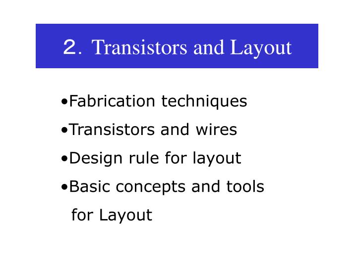
2. Transistors and Layout. Fabrication techniques Transistors and wires Design rule for layout Basic concepts and tools for Layout. 2.2 Fabrication Processes 2.2.1 Overview. Minimum channel length=0.5μm λ=0.25μm ---- 0.5μProcess. 2.2.2 Fabrication Steps. Photoresist:

E N D
2.Transistors and Layout • Fabrication techniques • Transistors and wires • Design rule for layout • Basic concepts and tools • for Layout
2.2 Fabrication Processes2.2.1 Overview Minimum channel length=0.5μm λ=0.25μm ---- 0.5μProcess
2.2.2 Fabrication Steps Photoresist: mask pattern SiO2 pattern • Features are patterned on the wafer by a photolithographic process; • The wafer is covered by light sensitive material “photoresist”. • It is exposed to light with proper mask pattern. • The patterns left by the photoresist can be used to control where SiO2 is grown on materials.
Steps in processing a wafer(twin tub process) • Put tubs into wafer. • Form an oxide covering on wafer and the polysilicon wires. • Diffusion (wires) (polysilicon masks the formation of diffusion wires.=self-aligned) • Metal connections are made with filling cuts (via) to make connections after another oxide layer is deposited.
2.3 Transistors2.3.1 Structures of Transistors • “MOS” : sandwich of Metal, Oxide, and Silicon (semiconductor substrate). • The positive voltage on the polysilicon forms gate attracts the elctoron at the top of the channel. • The threshold voltage (Vt) collects enough electrons at the channel boundary to form an inversion layer (p -> n). Field Oxide Gate Oxide
Layout of n-type and p-type transistors nMOS pMOS nMOS with wide width
2.3.2 A Simple Transistor Model Linear region Saturated region
2.3.3 Transistor Parasitics • Cg: gate capacitance = 0.9fF/μm2 (2 μprocess) • Cgs/Cgd: source/drain overlap capacitance =Cox W (Cox: gate/bulk overlap capacitance)
2.2.4 Tub Layout and Latchup • Tub Ties (substrate bias)
2.2.5 Advanced Transistor Characteristics Parallel plate oxide capacitance per unit area Cox = εox/xox where εox= permittivity of silicon dioxide = (3.9 εo) xox = oxide thickness
Shape of the inversion layer as a function of gate voltage • Q(y)=Cox(Vgs-Vt-Vy) • dV=Iydy/μQ(y)W
2.4 Wires and Vias • Wires of different layers are insulated by an additional layer of SiO2. • Vias are cuts in the insulating SiO2.
MTF for metal wires • The mean time for failure (MTF) MTF=j-ne(Q/kT). j:current density n:constant(1~2) Q:diffusion activation energy. • jMetal < 1.5mA/μm width (4.5mA by 3μm width wire)
2.4.1 Wire Parasitics Cj0 = εSi/xd Depletion region capacitance Cj0 : zero-bias depletion capacitance εSi : permittivity of silicon xd : thickness of depletion region depending on applied voltage.
metal 3 0.1fF/cm2 0.3fF/cm2 (overlapping area) Depending on distance
Example of Parasitic capacitance measurement 0.5 μm process (λ=0.25 μm) 1) Unit bottomwall capacitance C1_0=0.6fF/μm2 Area=3 μm x 0.75 μm+1.0 μm x 1.0 μm=3.25 μm2 (3.25 λ2μm2) C1=0.6fF(/ λ2) x 3.25 (xλ2)=1.95 fF 2)Unit sidewall capacitance C2_0=0.2fF/μm Perimeter=0.75+4+1+1+0.25+3=10 μm C2=0.2fFx10=2fF 3) Metal capacitance C3_0=0.04fF/ μm2 Area=2.5 μm x 1.5 μm=3.75μm2 C3=0.04fFx3.75=0.15fF 4) Metal fringe capacitance C4_0=0.09fF /μm Perimeter=(2.5+1.5)x2=8 μm C4=0.09fFx8=0.72fF 5) Total capacitance=1.95+2+0.15+0.72=4.85fF
Example of Resistance Measurement • Ohms per square [Ω/ ] = Sheet resistance • 0.5 μm process (λ=0.25 μm) • Polysilicon resistance • Rpoly=[18/3]x4[Ω/ ]=24 Ω • n-diffusion resistance • [(9/3)+(6/3)+1/2]x • 2 [Ω/ ]=11 Ω
2.5 Design Rule2.5.1 Fabrication Errors • Problems when wire are too wide or narrow. • Polysilicon should extend beyond boundary of difusion area. • The cut of via must connect elements and not mistakenly connect to substrate or others.
2.5.2 Scalable Design Rules All physical parameters to be shrunk by a factor 1/x • Lengths: W–› W/x • Widths: L –› L/x • Vertical dimensions such as oxide thickness: tox–› tox/x • Doping concentrations: Nd –› Nd/x • Supply voltages: VDD-VSS –› (VDD-VSS) Id’/Id =1/x Cg’/Cg =1/x (C’V’/I’)/(CV/I) = 1/x
2.5.2 SCMOS Design Rules • Metal1 min-width=3λ, min-sep= 3λ • Metal2 min-width=3λ, min-sep= 3λ • poly min-width=2λ, min-sep= 2λ • n, p-dif min-width=3λ, min-sep(n-n, p-p)= 3λ (n-p 10λ) • Tube min-width=10λ, min-distance(tub- active)= 5λ • Transistors min-W/L=3λ/2λ poly extension= 2λ dif extension= 2λ active-poly/metal via=λ min-sep(tran.-tran.)= 2λ min-sep(tran-tub.tie) = 3λ
SCMOS Design Rules (continue) • Vias cuts=2λx2λ via =4λx4λ n,p.diff-poly, poly-metal1 n,p.diff-metal1, metal1-metal2 • Tub ties cuts =2λx2λ metal =4λx4λ • Metal1 min-width=6λ, min-sep= 4λ available via to metal2 • Special rules cut to poly – poly sep =3λ poly.cut-dif.cut sep=2λ cut-tran.active sep =2λ dif.cut-dif sep = 4λ meta2.via must not be directly over polysilicon • Prohibit small negative features.
2.6 Layout Design and Tools2.6.1 Layouts for Circuits • Net: a set of electrical connections • Wire: a set of point-point connections. • Wire segment: a straight section of wire. • Circuit schematic: n-type, p-type transistors with W/L
2.6.4 Layout Design and Analysis Tools • Layout Editors: intensive graphic program for manual layout symbolic layouts: more detail than stick diagram • Design Rule Checkers (DRC): check items: minimum spacing minimum size combination of layers • Circuit Extractions: extension of DRC (identify transistors and vias) a complete job of compnents and wire extraction to produce a net list from layout.
Circuit Extraction Basic Operation of Circuit Extraction NOT, AND, OR between 2 masks grow and shrink operation over masks. 1) extraction of transistors AND(poly - p/n.diff) 2) identify via grow cut AND(grown-cut, metal, poly)
Hierarchical Circuit Extraction • Flattening is required to make extracted netlist small by making correspondence between net names in cells and nets int the top-level components.
2.6.5 Automatic Layout Cell generator (or macrocell generator) parameterized layout
Standard Cell Placement and Routing Logic gates, latches, flip-flops, or larger logic Routing channels
An Example of Standard Cell Layout • 2 stages placement routing