Download
1 / 41
410 likes | 605 Views
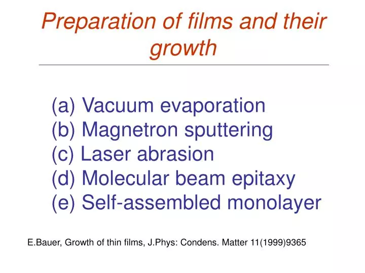
Preparation of films and their growth. (a) Vacuum evaporation (b) Magnetron sputtering (c) Laser abrasion (d) Molecular beam epitaxy (e) Self-assembled monolayer. E.Bauer, Growth of thin films, J.Phys: Condens. Matter 11(1999)9365. Schematic drawing of the evaporation chamber.

E N D
Preparation of films and their growth (a)Vacuum evaporation (b) Magnetron sputtering (c) Laser abrasion (d) Molecular beam epitaxy (e) Self-assembled monolayer E.Bauer, Growth of thin films, J.Phys: Condens. Matter 11(1999)9365
Thermal evaporation and the uniformity of deposits • The simplest technology, raising the temperature of the source materials; • An open boat, suspended on a wire; • The boat or wire is a high temperature material, such as W or Mo and must not react with the evaporant; • The substrate hold should be rotated in order to get uniform deposits; • The deposition rate is determined by the source area temperature and the distance between the source and substrate as well as the evaporant itself; • Electron beam deposition for high temperature materials or materials which interact with the crucible.
Binary alloy evaporation dZA / dZB = (MB/MA )1/2 exp[-(ΔHA- ΔHB)/RT] (CA/CB) = K (CA/CB). MA, MB are the mass of A and B element; ΔHA and ΔHB the evaporation heat, CA : CB is the atomic ratio.
(the ratio of A:B) (K) The variation of the ratio of evaporated A and B element in binary alloy with time
Sputtering and ion beam assisted deposition Sputtering (Ion beam assisted deposition (IBAD), Ion beam sputter deposition (IBSD)) provides the better quality deposits: • at low substrate temperature, thus avoiding large scale interdiffusion, • adhere well to the substrate, • to realize a reactive sputtering.
The sputtering rate for the different element (using 500 eV Ar+).
Pulsed laser width 10-20 ms, Density 1-5 J/cm2 Schematic picture of Laser ablation
• A continuum NY81-C Nd:YIG laser • The wavelength, pulse frequency and pulse width are 355 nm, 10Hz and 10ns, respectively • The focused laser beam with the energy density of 3-4 J/cm2 • Ceramic target • The distance between the target and substrate is 55 mm • 3x10⁻⁵mTorr before introducing pure O2 • O2 gass flow of 60 sccm at a pressure of 75 mTorr • After deposition, the amorphous film is post annealed for 2 minutes at 650oC in air
Summary (1)The chemical composition of the film is the same as that of target (2) The polycrystalline films on ceramic glass substrate have easy magnetization axis normal To the film surface, nanometer size grain and very smooth surface (3) The film shows high squareness of Faraday hysteresis loop (4) Magnetization of the film at temperature range from 240K to 340K is almost temperature independent.
The special points of Pulse Laser Ablation The advantages • The ablated sample with the same composition as the target composition; • High energy particles is beneficial for the film growth and realizing a chemical reaction on substrate; • Reaction deposition; • Multilayers growth and thickness control precisely. The disadvantages • Formingsmall particle, 0.1-10 µ m, • thickness deposited is not uniform
Advantages of MBE • Growth under controlled and monitored conditions with in • situ analysis of film structure and composition (RHEED, • LHEED, XPS, AES). • (2) A key advantage of MBE is that it enables growth of the • layered structure along specific crystalline direction; • (3) Lattice-matching between the seed film (prelayer) and • substrate can be achieved by appropriate choice of materials • and the growth axis of the magnetic structure selected.
Magnetic hysteresis loops for oriented Co-Pt super- lattice recorded by MO effect.
Thin film growth Schematic representation of the three growth modes (a) Island (b) layer-plus-island (c) layer by layer. Substrate The change of AES peak with The deposition deposite ML
Two arrangements for four deposited atoms in the same phase epitaxy 7 AA bonds 8 AA bonds (stable state)
In the case of the same phase epitaxy, the stable state is one- Layer-arrangement, namely, two demitional growth.
For the different phase epitaxy (a) -4uAB – 12uAA -8uAB-10uAA (b) If uAA > 2uAB the case of (a) is beneficial for the reduction of energy
The condition for double layers arrangement (Island): • N=8, uAA>2uAB, (b) N=18, uAA>1.5uAB, (c) N=32, • uAA>1.33uAB, (d) N=50, uAA>1.25uAB, (e) N=72, uAA> • 1.24 uAB.
Other factors should be considered • The size of the epitaxy atoms • If the size of A atom (epitaxy) is larger than that of B • (substrate), a compressive strain appears in the epitaxy • layers, conversely, tensile force appears; • (b) The strain increases with the increase of epitaxy • thickness and finally dislocation could exist; • (c) Island appears if the size A atom is largely different from • B atom (substrate).
Electron-based techniques for examining surface and thin film process AES (Auger electron spectroscopy) LEED (Low energy electron diffraction) RHEED (Reflection high energy electron microscopy) TEM (Transmission electron microscopy) REM (Reflection electron microscopy) STM (Scanning tunneling microscopy) AFM (Atomic force microscopy) PEEM (Photoemission microscopy) SEM (Scanning electron microscopy) SNOM (Scanning near field optical microscopy) XPS (X-ray photoemission spectroscopy) UPS (Ultra-violet photoemission spectroscopy)
Auger Electron Spectoscopy (AES) Si KL1L2,3 transition Si KLL Auger scheme (Chang Surface Sci., 25(1974)53).
High resolution AES spectrum of Ge LMM for 5KV incident energy. The strongest peaks, within the L2M4,5M4,5 series at 1145 and L3M4,5M4,5.
The surface AES of Fe The integrating spectroscopy, N(E), of the surface AES, and N’(E)=dN(E)/dE.
Photoelectron Spectroscopies: XPS and UPS After the electron at inner shell or valence electron absorb photon energy, they leave atom and become photo-electron, Ek = hv – Eb, where, hv photon energy, UPS uses ultra-violet radiation as the probe and collects electrons directly from the valence band, XPS excites a core hole with X-rays and collect binding energy of the electrons at the inner cells.
XPS The electron energy spectrum on Ni obtained by bombardment of 1.25Kev photon.
Scanning Tunneling Microscopy(STM) • The tunneling current is measured by W needle • The distance between the tip and sample surface is below 1 nm; resolution along vertical is 0.01nm and in transverse is 0.1nm • The tip is applied a few voltage and the tunneling current is 0.1 to 1.0 nA • The current is related not only to the height of atom on the surface, but also to the atomic density (density state)
Atomic Force Microscopy (AFM) STM is only applied to observe surface for conductor or semi- conductor, while AFM is an appropriate tool for all samples. The reflect light place is 3-10nm after the height of tip changes 0.01nm. • Three operation models of AFM: • contact (2) non-contact (3) • tapping model.
Transmission electron microscopy (TEM) • With TEM one can obtain diffraction patterns and images • of the sample, revealing microstractural defects such as • dislocation, grain-, twin- and antiphase boundaries • (2) In order for the electrons to pass through the specimen, • it has to be electron transparent (hundreds of nm) • (3) High resolution than a light microscope
Atoimic resolution TEM image of a Co doped TiO2 film. No segregation of impurity phases was obser- ved in the film.