Download
1 / 1
10 likes | 123 Views
Making Electronic Devices from the World’s Thinnest Material High-yield processes suitable for mass fabrication, DMR-0520404.

E N D
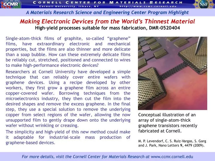
Making Electronic Devices from the World’s Thinnest MaterialHigh-yield processes suitable for mass fabrication, DMR-0520404 Single-atom-thick films of graphite, so-called “graphene” films, have extraordinary electronic and mechanical properties, but the films are also thinner and more delicate than a soap bubble. How can these extremely delicate films be reliably cut, stretched, positioned and connected to wires to make high-performance electronic devices? Researchers at Cornell University have developed a simple technique that can reliably cover entire wafers with graphene devices. Using a recipe developed by other workers, they first grow a graphene film across an entire copper-covered wafer. Borrowing techniques from the microelectronics industry, they then cut the film into the desired shapes and remove the excess graphene. In the final step, they use a special solution to remove the underlying copper from select regions of the wafer, allowing the now unsupported film to gently drape down onto the underlying wafer without wrinkling or creasing. The simplicity and high-yield of this new method could make it adaptable for industrial-scale mass production of graphene-based devices. Conceptual illustration of an array of single-atom-thick graphene transistors recently fabricated at Cornell. M. P. Levendorf, C. S. Ruiz-Vargas, S. Garg and J. Park, Nano Letters 9, 4479 (2009). For more details, visit the Cornell Center for Materials Research at www.ccmr.cornell.edu


![Dean C. Hines [Deputy Principle Investigator]](https://cdn2.slideserve.com/4759340/slide1-dt.jpg)