Download
1 / 16
180 likes | 387 Views
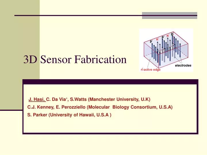
3D Sensor Fabrication. J. Hasi, C. Da Via ’ , S.Watts (Manchester University, U.K) C.J. Kenney, E. Perozziello (Molecular Biology Consortium, U.S.A) S. Parker (University of Hawaii, U.S.A ). STANFORD NANOFABRICATION FACILITY.

E N D
3D Sensor Fabrication J. Hasi, C. Da Via’, S.Watts (Manchester University, U.K) C.J. Kenney, E. Perozziello (Molecular Biology Consortium, U.S.A) S. Parker (University of Hawaii, U.S.A )
STANFORD NANOFABRICATION FACILITY All the fabrication work is performed at Stanford Nanofabrication Facility in the CIS building, which was completed in 1985. SNF encompasses 10,000-sq.ft, and has dedicated space designed specifically to support state of the art processing.
FABRICATION Chris Kenney, Jasmine Hasi, Eric Perozziello -32 3E ATLAS Single Chips -6 4E ATLAS Single Chips -6 2E ATLAS Single Chips -Quarter Size ATLAS Chips -ATLAS Test Structures -Other structures P-type, 4” wafers, 12.5kΩ-cm, (1-0-0), float-zone wafers, 200 + 25 microns thick Yield on one wafer ~80% (Yield definition only means that all electrodes could be biased without drawing abnormal currents )
4E 2E 3E 50 mm 50 mm 50 mm 400 mm 400 mm 400 mm n n n p p p 71 mm 103mm 56 mm Vfd ~20V Vfd ~8V Vfd ~5V 3D Electrode Configuration Cinzia Da Via’ Slide
KEY STAGES THAT MAKE THIS TECHNOLOGY POSSIBLE 3D process consists of > 100 steps • WAFER BONDING (mechanical stability). After complete processing this support wafer will be removed. 2. PHOTOLITHOGRAPHY 3. MAKING THE HOLES 4. FILLING THE HOLES 5. DOPING THE HOLES AND ANNEALING 6. METAL DEPOSITION
PHOTOLITHOGRAPHY Photolithography encompasses all the steps involved in transferring a pattern from a mask to the surface of the silicon wafer • Clean wafers • Deposit barrier layer e.g.SiO2, metal etc. • Coat with photoresist • Soft bake ( 90°C for a minute) • Align masks (square glass plate with a patterned emulsion or metal film) • Expose pattern • Develop photoresist • Hard bake (110°C for a minute) • Etch windows in barrier layer • Remove photoresist
MASK DESIGN • Mask Layers • P ox (open the P windows in the oxide and nitride layer) • P holes ( defines region for p electrodes) • N ox (open the N windows in the oxide and nitride layer) • N holes ( defines region for n electrodes) • Metal • Glass (vias in protective layer) • Dice ( separate individual die) Mask design for the 3D process run designed by C.J. Kenney using CADANCE.
MAKING OF THE HOLES Deep, reactive–ion etchings to produce HIGH ASPECT RATIO of over 18:1, near vertical holes. The fabrication of 3D structures depends on the capability of etching narrow holes with high precision in the silicon bulk. Deep reactive ion etching has been developed for Micro-Electro-Mechanical Systems (MEMS). Photo of the plasma (violet colour) from the porthole of the STS (Surface Technology Systems) while etching a silicon wafer
ASPECT RATIO d Aspect Ratio D:d D SEM profile of a silicon wafer (thickness of 525μm) with 14μm diameter etched holes of an aspect ratio of ~ 15:1. SEM profile of a ~10μm etched trench and a 10μm etched hole.
PLASMA ETCHING BOSCH PROCESS: alternating passivating (C4F8) and etch cycles (SF6); • Within the plasma an electric field is applied perpendicular to the silicon surface. • The etch cycle consists of fluorine based etchants which react with silicon surface, removing silicon. The etch rates are ~1-5μm/minute. • To minimise side wall etching, etch cycle is stopped and replaced with a passivation gas which creates a Teflon-like coating homogenously around the cavity. Energetic fluorine ions, accelerated by the e-field, remove the coating from the cavity bottom but NOT the side walls.
FILLING AND DOPING THE HOLES The holes can be filled with doped gas molecules at low pressure and moderate temperatures to form p & n electrodes within the detector. • POLYCRYSTALLINE SILICON IS DEPOSITED IN A LOW PRESSURE CHEMICAL VAPOUR DEPOSITION (LPCVD) USING A THERMAL DECOMPOSITION OF SILANE. • DOPED WITH EITHER BORON OR PHOSPHOROUS TO PRODUCE EITHER N OR P-TYPE ELECTRODES 2P2O5 +5 Si-> 4P + 5 SiO2 2B2O3 +3Si -> 4 B +3 SiO2 • ANNEALING FOLLOWS, IN WHICH THE DOPANTS ARE DIFFUSED INTO THE SURROUNDING SINGLE CRYSTAL SILICON FORMING PN JUNCTIONS
POLY-FILLED AND DOPED ELECTRODE Cross section of an electrode of a 27μm through a 180μm thick silicon wafer, had 0.6 microns of poly deposited on its inner surface, its surface heavily doped with boron and then had the remaining hole filled with poly via LPCVD. Silane (SiH4), which has a low sticking probability at 625°C, bouncing thousands of times before “sticking “, producing a conformal coating
PLASMA DICING-ACTIVE EDGES • Active Edge is an edge electrode located at the perimeter of the whole device • Using the same electrode process but for the full edge of the device, eliminates large dead regions • Tiling these sensors together will produce large seamless detector area • NO SAWING NECESSARY ! • No chips or cracks • Arbitrary edge shapes
METAL DEPOSITION Metal films deposited to electrically interconnect pixels • The substrate is first covered with an insulating film (oxide) through which the windows are etched to allow the metal to make contact with the substrate. • The metal is then deposited and patterned into strips connecting desired elements and making good electrical contacts with the silicon. Because the electrodes are already doped p+ /n+ contact between electrode and metal is ohmic. Photo of a section of one of the completed 3D devices (NOT FP420) showing the connections of the aluminum strips to the electrodes The material that we used was aluminum (1% silicon). Resistivity of about 2.7 µΩ-cm
FABRICATION YIELD • Due to extreme topography on the wafer surface (e.g. poly-filled holes), it makes it difficult to spin on a uniform layer of photoresist, which is a critical step repeated many times. • When plasma etching either holes, edges etc., the use of thick resist is required, however, high-viscosity resists seem to have more particulates and clumps of resist associated with them. • Mechanical fractures can occur during the plasma dicing or fusion bonding steps. • When patterning the metal, some aluminum contact strips would etch away. Defect caused by bubbles in the resist Shorts between the n and p electrodes caused by the resist not being fully exposed due to the greater thickness or the presence of a foreign material.
CONCLUSION: IMPROVING THE YIELD The major changes to improve yield were to: • Add process-checking yield steps into the process run, change chemicals, do at least two spins on the spin dryer, wear face shield to reduce particle generation etc. • Carefully inspected the wafers after every litho step and re-spun the wafers if necessary • For the thick resist used for the trench etch, we covered resist defects with polyimide tape • We filled the trenches with poly, etched the poly off the top surface and then repeated the fill and etch procedure again in an effort to better fill the trenches • We widened the plasma dice lane from 50 microns to 120 microns to avoid mechanical chips. • Widened the aluminium contact strips • Start more wafers than needed, and hold back some of them part-way through the process