Download
1 / 31
380 likes | 687 Views
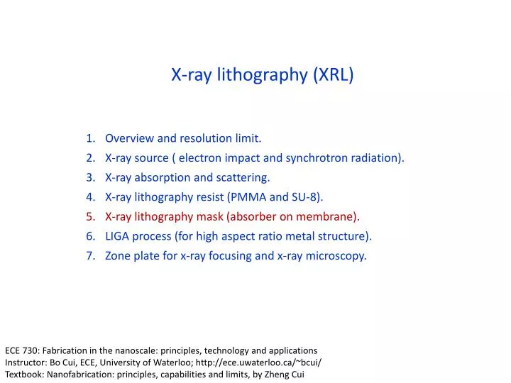
X-ray lithography (XRL). Overview and resolution limit. X-ray source ( electron impact and synchrotron radiation). X-ray absorption and scattering. X-ray lithography resist (PMMA and SU-8). X-ray lithography mask (absorber on membrane). LIGA process (for high aspect ratio metal structure).

E N D
X-ray lithography (XRL) Overview and resolution limit. X-ray source ( electron impact and synchrotron radiation). X-ray absorption and scattering. X-ray lithography resist (PMMA and SU-8). X-ray lithography mask (absorber on membrane). LIGA process (for high aspect ratio metal structure). Zone plate for x-ray focusing and x-ray microscopy. ECE 730: Fabrication in the nanoscale: principles, technology and applications Instructor: Bo Cui, ECE, University of Waterloo; http://ece.uwaterloo.ca/~bcui/ Textbook: Nanofabrication: principles, capabilities and limits, by Zheng Cui
X-ray lithography: mask membrane materials • X-ray mask membrane materials: • Thin (1-2m) membranes from silicon, silicon nitride, boron nitride, titanium or diamond, for high resolution (<100nm) using longer wavelength (few nm). Very difficult to make and fragile. • Thick (>100m) “sheets” from graphite, beryllium or kapton (polyimide), for high aspect ratio (low resolution >1m, LIGA process) using shorter wavelength (<5Å). • Requirement: • Good x-ray and optical (for alignment) transmission • Compatible with plating of Au absorber • Radiation resistant • Good mechanical stability, low internal stress (no bending or deformation) • Good thermal conductivity (no overheating) • Compatible with established mask making processes and equipment Absorber Structure Membrane Optical image of a mask Mask Frame
Popular membrane materials Beryllium (Z=4): best transmission, thick sheets possible, good thermal conductivity but: toxic, no optical transparency, expensive. Rigid graphite (Z=6): acceptable transmission, thick sheets possible, good thermal conductivity, cheap. but: poor surface roughness and no optical transparency (difficult for alignment). Diamond (Z=6): acceptable transmission, good thermal conductivity, optical transparency but: free-standing in bigger format critical, expensive. Silicon based (Si, SiC, Si3N4 Z=14): acceptable transmission, optical transparency, established MEMS material but: thin membrane, poor cooling properties, fragile Titanium (Z=22): acceptable transmission but: thin membrane, poor cooling properties, no optical transparency Lower Zhigher transmission Kapton is polyimide
X-ray mask: absorber (high Z material Au, W, Ta) Transmission through Au of different thickness Linear absorption coefficient of Au (1/m) 2m 10m 20m 50m 1.24Å For 10keV, need Au >10m thick for <10% transmission, can be done by Au electroplating, yet difficult to have high resolution (<<1m). For 1kV (1.24nm), need m/9=110nm in order to have transmission =1/e=37%.
Various x-ray masks: Ti and Si “membrane” X-ray mask – Ti thin film membrane X-ray mask – silicon substrate Pattern area (6.5 x 2.5 cm2) Ti mask: FZK IMT 100μm thick Si wafer, 30μm of Au absorber Thick Au is needed to prevent exposure in blocked area when using thick (mm) resist for high aspect ratio resist structure. Thick resist requires short wavelength (less absorption in resist and Au) and high dose in order to fully expose resist bottom.
Patterning absorber: high resolution fine features by e-beam lithography Here SiC is used, instead of Si3N4 For high resolution, longer wavelength (higher absorption) is desirable, to allow thin absorber and thin membrane/resist. RIE Au? Perhaps W of Ta Cerrina, J Phys D, 2000
KOH etching of single crystal silicon is anisotropic • The etching rate R: R(111)<<R(110)<R(100), R(111)/R(100)few 100. Basically, the denser the crystalline plane, the lower the etching rate. (111) plane is densest (more Si atoms per unit area). • The etching rate of SiO2 is about 1/1000 that of R(100), so SiO2 can be a good etching mask. • However, for wafer-through etching (etch 0.5mm), better use Si3N4 as etching mask, whose etching rate in KOH is negligible. • Typical etchant contains 20-50% KOH in water at temperature 50-90oC (room temperature is also OK, but etch much slower, need days to etch through 0.5mm-thick wafer). (1,1,0) (-1,1,1) (-1,1,-2) High aspect ratio Si grating Silicon nitride membrane Si (110) wafer (NOT (100)) (100) LPCVD silicon nitride (100) Si wafer Silicon (100) (111) The angle between (111) and (100) is cos=1/3, so =54.74o.
X-ray lithography (XRL) Overview and resolution limit. X-ray source ( electron impact and synchrotron radiation). X-ray absorption and scattering. X-ray lithography resist (PMMA and SU-8). X-ray lithography mask (absorber on membrane). LIGA process (for high aspect ratio metal structure). Zone plate for x-ray focusing and x-ray microscopy.
LIGA: introduction • LIGA: LIthographie Galvanik Abformung. (German name) • It is a fabrication process for high aspect ratio (height/width) microstructures consisting of three major process steps. • X-ray lithography (LI=lithographie) to generate primary microstructures. Nowadays similar process but using other lithographies is also called LIGA. • Electroplating (G=Galvanik) to produce molds in metals such as Ni. • Molding (A=Abformung) using the metal mold to batch produce secondary microstructures in polymers, metals, ceramics… First publication on LIGA appeared in 1982. Today, more and more prototypes are fabricated by LIGA. Some LIGA companies have been founded to provide professional services to users
Why is LIGA interesting • Very high aspect ratio (height : width > 100 : 1) structures can be achieved. • Have more material selectivity in final products (metal, polymer or even ceramics). • Vertical and better surface roughness in sidewall • Vertical sidewall slope < 1μm/mm • Surface roughness <30-50nm (peak to valley) • It can be applied in both MEMS and traditional precision manufacturing. Patterning accuracy – DXRL (deep XRL, few Å) Patterning accuracy – UDXRL (ultra-deep x-ray lithography, <1Å) Ph.D. Thesis Jürgen Mohr, IMT/FZK, 1987 Ph.D. Thesis Sven Achenbach, IMT/FZK, 2000
LIGA problems • X-ray source (synchrotron radiation) very expensive. • Long time exposure and develop. But SU-8 is >100 faster than PMMA. • Other competing technology are rapidly catching up: LIGA-like process using UV lithography with SU-8 resist (see below); deep silicon etching capable of etching through a 0.5mm Si wafer with vertical sidewall. Structure by photolithography (NOT x-ray lithography) in SU-8, a negative tone photoresist (and x-ray, e-beam resist). (A) SEM image of honeycomb structures with designed sidewall width of 6m and a height of 2000m. The micro-feature next to the honeycombs is an Arabic number “6” with designed width of 7m and a height of 2000m. (aspect ratio 2000:7 ) (B) Micro-comb structures with designed thickness of 40m and height of 2000m. “A numerical and experimental study on gap compensation and wavelength selection in UV-lithography of ultra-high aspect ratio SU-8 microstructures”, Wang, Sensors and Actuators B, 2005.
Why optical lithography can have high resolution (7m) in so thick resist (2000 m)? SU-8 is a negative resist • The SU-8 resist profile after development should be wider at the bottom (by x). • But the bottom is less exposed due to absorption of x-ray. So bottom can be actually narrower. • (In the extreme situation, no exposure at bottom, then the width at resist bottom should be 0 after development) • A well balance between the two trends can lead to a vertical sidewall for very high aspect ratio structure. • In addition, here the pattern is isolated. There is no physical limit of feature size for isolated pattern. For dense grating pattern, the HP (half pitch) will be limited by the R given above. g Resist (SU-8) t g: gap t: thickness x (R)
Applications of LIGA: MEMS LIGA Acceleration Sensor PMMA structure Ni - structures 120 μm high Detail Redundant Sensor System MEMS: Micro-electro-mechanical systems
3D structure fabrication by LIGA (using multiple exposures with rotation)
3D structure fabrication by LIGA (using PMMA and SU-8 stack) PMMA won’t be exposed at doses sufficient for exposing SU-8 Here SU-8 is already cross-linked, thus won’t be affected by further exposure to x-ray.
X-ray lithography (XRL) Overview and resolution limit. X-ray source ( electron impact and synchrotron radiation). X-ray absorption and scattering. X-ray lithography resist (PMMA and SU-8). X-ray lithography mask (absorber on membrane). LIGA process (for high aspect ratio metal structure). Zone plate for x-ray focusing and x-ray microscopy.
How zone-plate works Maximum light intensity at the focal point if the light from each non-blocked zone interfere constructively (“in-phase”). Zone 1 2 3 4 5 6 7 8
Fresnel lenses (zone plates): overview • There is only reflection optics for soft x-ray and no optics for hard x-ray. • Zone plate is the only option for focusing and imaging in this wavelength range. • Number of zones is up to 10000-20000, materials – Au, Pt and other heavy metals. • Width of the outmost zone (i.e. spatial resolution) can be as small as 15nm, and the radius of zone plates is up to 2mm. • Most zone plate is fabricated by e-beam lithography, followed by electroplating of heavy metals into the trenches in resist, with aspect ratio limited to about 1:10. High aspect ratio metal pattern by EBL and electroplating Zone-plate schematic.
Zone-plate equations The area between r1 and r2 is transparent, that between r2 and r3 is blocked, that between r3 and r4 is transparent… Here we assume r1 is such that the distance from r1 to focal point is f+/2. n=1, 2, 3……N Assume N<<f D2rN r: outermost zone width R: resolution Those equations are good for the case of N<<f, which is equivalent to small NA. NA is always small for hard x-ray, but less so for soft x-ray zone plates. The area of each zone is (rn2-rn-12)=f=constant, so each zone contributes equally to the intensity at focal point.
Zone-plate is indeed a lens Try your best to understand this slide. It won’t be included in exams We know that for a regular optical lens, the equation is Therefore, a zone plate is like a lens, with magnification equal to p/q. independent of n for rn=(nf)1/2, which is the same as before. David Attwood, “Soft x-rays and extreme ultraviolet radiation”, Cambridge University Press.
Zone plate fabrication: e-beam lithography + electroplating Zone plate with 100nm-thick gold with a 30nm outer zone width and 300 zones. It is used to form the image on the right side with 30nm resolution.
Focusing x-ray: zone plate array lithography It seems that only MIT, where x-ray lithography is invented, is still working on this topic. Now a hot research area is x-ray imaging using zone-plate optics.
Other application of zone plate: x-ray (including soft x-ray, i.e. EUV) microscopy
X-ray imaging - highest resolution achieved This microscope covers a spectral range of 250eV (5nm) to 1.8keV (0.7 nm), so that primary K and L atomic resonances of elements such as C, N, O, Al, Ti, Fe, Co and Ni can be probed. Best spatial resolution achieved: 15nm lines. Sub-10nm is on the way. Outer zone-width=15nm, Au is 80nm thick. Zone plate fabrication is the most challenging task for x-ray microscopy W. Chao, ... David Attwood, “Soft X-ray microscopy at a spatial resolution better than 15 nm”, Nature 435, 1210-1213 (2005).
Application in bio-imaging 2.3nm Absorption length for soft x-rays in water and a generic protein as a function of photon energy. Natural contrast in the water window, between the carbon and oxygen absorption edges, where the high carbon content protein is absorbing where water is relatively transparent. Imaging of thicker objects (10m, size of typical mammalian cells) requires operation in the lower part of the water-window where the transmission is higher, such as =2.4nm from synchrotron radiation or N2 laser-produced plasma.
X-ray absorption: photoelectric absorption dominates at <10keV The picture below is similar to electron bombardment x-ray source (see slide #14), where core electron is kicked off by an incident electron. Here it is kicked off by x-ray (the incident x-ray is absorbed/lost). In the relaxation process, the lower (than incident x-ray photon) energy photon is a fluorescent x-ray, while the lower energy electron is an Auger electron. (fluorescent x-ray) Photon (x-ray) (Auger electron) 1. A high energy x-ray photon impinges on an atom Electron (low energy) X-ray Photon (fluorescent x-ray) atom 3. The atom relaxes toits ground state byemission of a photon or electron Photo-electron 2. An inner-shell (here K-shell) electron (photo-electron) is knocked out of the atom. Auger-electron Electron (Auger electron, emitted from M-shell) k is the energy level of the K-shell…
Malaria infected red blood cells =2.4nm from bending magnet synchrotron radiation at ALS (Berkeley). Image resolution: 40nm Uninfected cell Newly infected cell 36 hours after infection. Image with visible light microscopy, for comparison. More photos at: http://www.cambridge.org/catalogue/catalogue.asp?isbn=9780521029971&ss=res Magowan C. et. al, “Intra-cellular structures of normal and aberrant plasmodium falciparum malaria parasites imaged by soft s-ray microscopy”, PNAS 94, 6222 (1997)
Soft x-ray images of Cryptosporidium Cryptosporidium is a common parasite found in lakes and rivers, and occasionally in municipal water supplies that may cause death. Images taken at 2.4nm wavelength The last of four sporozoites still in its protective oocyst. A sporozoite emerging from the oocyst
Liquid-nitrogen-jet laser-plasma source for compact soft x-ray microscopy Along with EVU source development, LPP (laser-produced plasma) source is becoming more popular for x-ray imaging, due to its compact size compared to synchrotron radiation. • Hydrogen-like and helium-like nitrogen ions emit strongly at =2.478nm (Ly-) and =2.879nm (He-), which is in the lower part of the water-window. • Nitrogen is relatively inert, with minimal debris contamination or damage. Jansson, “Liquid-nitrogen-jet laser-plasma source for compact soft x-ray microscopy”, Review of scientific instruments 76, 043503 (2005).