Download
1 / 18
180 likes | 342 Views
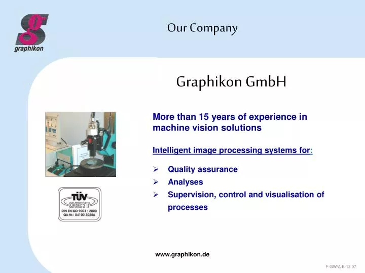
Our Company. Graphikon GmbH. More than 15 years of experience in machine vision solutions Intelligent image processing systems for :. Quality assurance Analyses Supervision, control and visualisation of processes. Graphikon GmbH. Long-Lasting Expertise in Machine Vision. The founding:.

E N D
Our Company Graphikon GmbH More than 15 years of experience in machine vision solutions Intelligent image processing systems for: • Quality assurance • Analyses • Supervision, control and visualisation of processes
Graphikon GmbH Long-Lasting Expertise in Machine Vision The founding: 1990 by Prof. Dr. Jürgen Saedler A team of competent specialists in the fields of system engineering, IT, mathematics, mechatronics, optical engineering, mechanical construction, sensor technology and control engineering The staff:
Graphikon GmbH Products • Tailor-made inline inspection systems with highest detection reliability • Stand-alone sorting machines with highest throughput • Offline / laboratory measurement systems with highest precision
Graphikon GmbH Turnkey Inspection Systems • G/WAFER for semiconductor industry • G/GLAS for glass industry • G/SOLAR for photovoltaic industry • G/INSPECT the construction kit for inspection solutions in the electronic, automotive, aviation and life science sectors
Graphikon GmbH References Electronics and Semiconductors : Epcos, Epigap, Infineon, OSA Opto, Siemens, Silicon Sensor Photovoltaics: DeutscheCell, ENfoton, Kyocera, Malibu Solar, Solarwatt, Solon, Würth Solar Automotive: Afag, Arcelor, Bosch, Brose, Corning, DaimlerChrysler, Eko Stahl, Elringklinger, Ina Schaeffler, Johnson Matthey, Lüdi, Porsche, Rasmussen, Salzgitter, Stüken, Takata-Petri, Trelleborg Sealing Solutions, Umicore, Volkswagen, Zehdenick Innovative Metall- und Kunststofftechnik, ZF Friedrichshafen Glass: Bystronic, Docter Optics, EG & G Heimann, Gat, General Electric, Gustav Brückner, Job, Osram, Philips, Rohmer + Stimpfig, Saint-Gobain Sekurit, Samsung, Schott
G/WAFER Wafer Inspection Microscope with coaxial bright field illumination, micropositioning system and high-resolution camera system for the evaluation of structures on wafers • Surface inspection of wafers up to 8“ in diameter • Recognition of particles down to a size of 2 microns, track bypasses and interruptions, mask defects and mask misalignment down to 0.7 micron • Fast teach-in for series inspection by highly efficient software tools • High throughput due to efficient analyses and innovative image acquisition methods with a continuously driven wafer
G/WAFER Wafer Inspection System Structure: • Stand: heavy measuring microscope MS 4 • 4-axis motion system • Telecentric lens system • Telecentric bright field illumination with flashing power LED • High-resolution 3-CCD colour camera
G/WAFER Wafer Inspection Optimum inspection results for: • Optoelectronic components • Sensor devices • Microsystems (MEMS) • ASICs • Power semiconductors • LEDs • Unstructured wafers • and more
G/WAFER Wafer Inspection Applications in several process steps: • Inspection of substrates • Supervision of single process steps • Final inspection of complete wafers • Final inspection of diced wafers
G/WAFER Wafer Inspection The Teaching Procedure: • Semi-automatic teach-in of a typical “good wafer” • Averaging of all dies • Masking-out of defects by sophisticated stochastic algorithms
G/WAFER Wafer Inspection The Teaching Procedure: • Calculation of ranges of assurance for every single pixel normal tolerances of appearance are taught in automatically • Semi-automatic labelling of structure areas • Definition of evaluating rules for single areas
G/WAFER Wafer Inspection The Inspection: • Automatic or manual wafer handling • Fully automatic alignment • Fully automatic scan image acquisition “on the fly” • Fully automatic balancing of colour variations of the wafer • Fully automatic focus control • Fully automatic pixel matching for every field of view
G/WAFER Wafer Inspection The Inspection: • Detection of deviations from the taught-in range of assurance • Evaluation of suspect structures according to the rule set • Automatic Defect Classification (ADC) by colour, position, size, shape and neighbourhood of objects • Marking of defective dies in the wafer map • Optional: Visual check of all detected defects / Offline Review
G/WAFER Wafer Inspection Typical defect types: • Scratches, particles • Holes / metallisation defects • Mask defects / mask misalignment • Bond pad defects/ improper probe marks • Defects at diced edges / chip-outs, misaligned dicing • Ink dots • Customer-specific defect types
G/WAFER Wafer Inspection The Options: • Alternative: Changeable magnifications for system resolutions from 5 microns down to 0.5 microns per pixel • Optional: Automatic change-over of magnification and illumination • Optional: Upgrade package for diced wafers on plastic foil • Optional: Inking of defective dies • Optional: Fully automatic wafer handling
G/WAFER Wafer Inspection The Throughput: • Depending from the chosen magnification the achievable inspection time is as shown in the chart: Defects down to: 2 µm 1.3 µm 4“ Wafer: approx. 4 min approx. 8 min 6“ Wafer: approx. 8 min approx. 15 min 8“ Wafer: approx. 16 min approx. 30 min
G/WAFER Wafer Inspection Flexibility: • Integration of the vision technology in other hardware environments (for instance PA200 test device) • Implementation of customer-specific inspection applications like dimensional checks, evaluation of edge quality and more
Graphikon GmbH Graphikon & Quasys A strong team for solving your inspection tasks