Download
1 / 25
250 likes | 393 Views
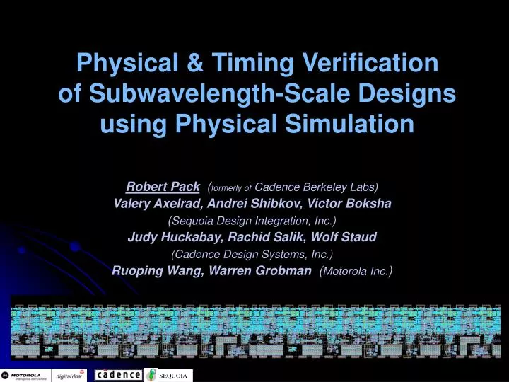
Physical & Timing Verification of Subwavelength-Scale Designs using Physical Simulation. Robert Pack ( formerly of Cadence Berkeley Labs) Valery Axelrad, Andrei Shibkov, Victor Boksha ( Sequoia Design Integration, Inc.) Judy Huckabay, Rachid Salik, Wolf Staud

E N D
Physical & Timing Verification of Subwavelength-Scale Designs using Physical Simulation Robert Pack(formerly of Cadence Berkeley Labs) Valery Axelrad, Andrei Shibkov, Victor Boksha (Sequoia Design Integration, Inc.) Judy Huckabay, Rachid Salik, Wolf Staud (Cadence Design Systems, Inc.) Ruoping Wang, Warren Grobman (Motorola Inc.)
Outline • Introduction • Problem Statement • OPE Impact on Device Performance • OPE and RET effects • Timing Analysis • Multi-partioning of critical devices • Summary
Introduction • DPI closure is key for successful <130nm designs • Current state-of-art EDA tools insufficient • insufficient in predicting performance • insufficient in predicting yield/reliability • Timing , SI, Race Conditions, Power… +/- %100 • These factors are responsible for costly fabrication yield re-spins – >%30 ! . Failure Costs are high! • Residual design-to-silicon distortions • Design and verification must account for increased process and device physics entanglement • Novel verification approach • unique new adjunct to DFM and MSO flows
Large % of flaws due to SI and Power • Parametric and Catastrophic Yield Loss • Feature Limited • Reliability Issue • Proximity Effects • Device • LITHOGRAHIC • Mitigation: OPC/PSM • Design Tools lack ability to capture complex physical effects Source: Kibarian/PDF Solutions & Collet Problem statement • Excessive Re-spins
FAIL! PASS ! Silicon Level Verification X Silicon - DRC Physical X Silicon - LVS Verification X Silicon - Timing FAIL! ü Layout - DRC ü Layout - LVS ü Layout - Timing Compares silicon to layout “Silicon Verification” must be performed before committing a SubWavelength design to silicon. Design Layout
Specific Problem: Silicon-Level VerificationIndustry focusing on Interconnects- OPE Impact on Device Performance
Verification of Process Proximity Effects - through physical simulation • OPE distortion affects transistor performance and matching • OPE distortion affects parasitics extraction accuracy • OPE is the major deterministic source of device variability • electrical impact of image quality • gate length variation • line end pullback • Complicates performance estimation / bin sort yield
OPE impacts • device performance characteristics • Vth • Idsat • Ioff • Power (leakage) • Yield/Reliability OPE is the major deterministic source of device variability
Experimental Simulation Conditions • 248nm • NA=0.7 • Source: • Binary and OPC • Pillbox; Sigma=0.6 • altPSM • Binary: Sigma=0.6 • PS: Sigma=0.35 • OPC Style: Aggressive Simulation-Based OPC • PSM Style: NTI Double Exposure altPSM • NOT A Motorola process • Not lithographically refined or RET optimized
Experimental Structure • 32-bit Adder scaled to 150nm • 4285 MOSFETs / CMOS technology • Lithography simulation performed full-structure K-T/Finle -Prolith
0.1-Def 0.2-Def 0.3-Def 0.4-Def 0.2-Def 0.3-Def 0.4-Def 0.1-Def Defocus EffectBIM – 0.1um steps BIM 0-Def
RET EffectsBIM,BIM+OPC,PSM+OPC BIM, 0-Def BIM, 0.3-Def BIM+OPC, 0.3-Def PSM+OPC, 0.3-Def BIM, 0.4-Def BIM+OPC, 0.4-Def PSM+OPC, 0.4-Def
BIM Timing Results • First Technique – (Rachid’s gate averaging) • Primarily a catastrophic Yield issue • Leakage from line end shortening not considered • Some transistors are outside of the model bounds SPICE Results
Electrical Analysis of Proximity Effects • Active devices (MOSFETs) responsible for circuit variability • Root cause of variability in sub-130nm mosfets is MOSFET geometry (CD control) • Geometry is the result of mostly deterministic effects and predictable Line-end pullback causes MOSFET leakage -> Yield Problem
Impact of Process Variation • Process variation causes image degradation • Defocus process window is important for manufacturability • Shown is the aerial image of the poly layer at increasing defocus • Gate length variation and line-end pullback cause MOSFET parameter variation and failure 0.2um defocus Defocus degrades image No defocus
Electrical Impact of Proximity Effects 0.15um defocus • Proximity effects cause distortion depending on shape and environment of features • Short poly segments (small mosfet W) print differently from long ones • Proximity of other gates impacts gate shape and electrical performance • Context of a mosfet must be considered when predicting its properties 0.2um defocus Defocus degrades image
MOSFET Variability and Yield MOSFET Gate Lengths MOSFET Idsat • Defocus causes the gate length distribution to widen and shift to shorter gates • Circuit failure results from strong MOSFET parameter variation • In extreme cases Source/Drain shorts (=very short gates) cause functional failure 0.1um defocus 0 defocus 0.1um defocus 0 defocus
Failure Outside Process Window Zero-length gates: Failures • Failure is observed as zero-length MOSFET by the verification tool • SPICE timing analysis confirms circuit failure in this case • Statistical analysis of MOSFET distribution across process window can be used to predict manufacturability 0.2um defocus MOSFET Gate Lengths
Conclusions • Current state-of-art EDA design and verification tools have insufficient predictive performance capability in the Nanometer Era – Timing , SI, Race Conditions… +/- %100 • These factors are also responsible in great part for costly fabrication re-spins – >%30 ! . Failure Costs are high! • Residual design-to-silicon distortions are a fact of life and must be accounted for in Nanometer Era • Design and verification tools must account for increased process and device physics entanglement. Verification must consider the impact of process proximity and process variation on circuit performance • Continuation of historical cycle, impact however is greater now than ever before • A novel verification methodology is proposed as a unique new adjunct to DFM and MSO flows to reduce costly re-spins and improve inherent design quality and manufacturability. Catch Potential Re-Spin Failures Before Mask and Silicon !
Acknowledgements • Thank you Chris and Ed at KLA-Tencor/Finle for RC Pack use of Prolith for ‘Gold-Standard’ confirmation and future work • Thank you Vinod and Fabio at Numerical Technologies for RC Pack use of IC Workbench for confirmation and future work
‘Naive’ Simulation-based OPC • Can make ‘pretty pictures’ on silicon but impact the real process window • At some level of k1, the context of the circuit and the device must be considered carefully • Many digital circuits are very forgiving of some levels of distortion.. but unforgiving of others • Analog circuits/devices have their own special consideration • Increased design-process integration care must be taken … it’s not just about making ‘pretty pictures’ on silicon • Judicious and minimal usage of OPC • Optimization target must be performance & Yield across Process-window.
Important issues for Designers, EDA, Maskmakers, lithographers, device designers, manufacturing… • Entanglement of traditionally separable entities. • The determination of which features are dimensionally and visually good enough must be done on the basis of the feature function and IC operational and manufacturing requirements. • Visual metrics are no longer sufficient • This era require new tools, new standards, new infrastructure….. • For EDA…It’s not just about wire RLC and parasitics
Acknowledgements • Thank you Chris and Ed at KLA-Tencor/Finle for RC Pack use of Prolith for ‘Gold-Standard’ confirmation and future work • Thank you Vinod and Fabio at Numerical Technologies for RC Pack use of IC Workbench for confirmation and future work